 3 months ago
10
3 months ago
10
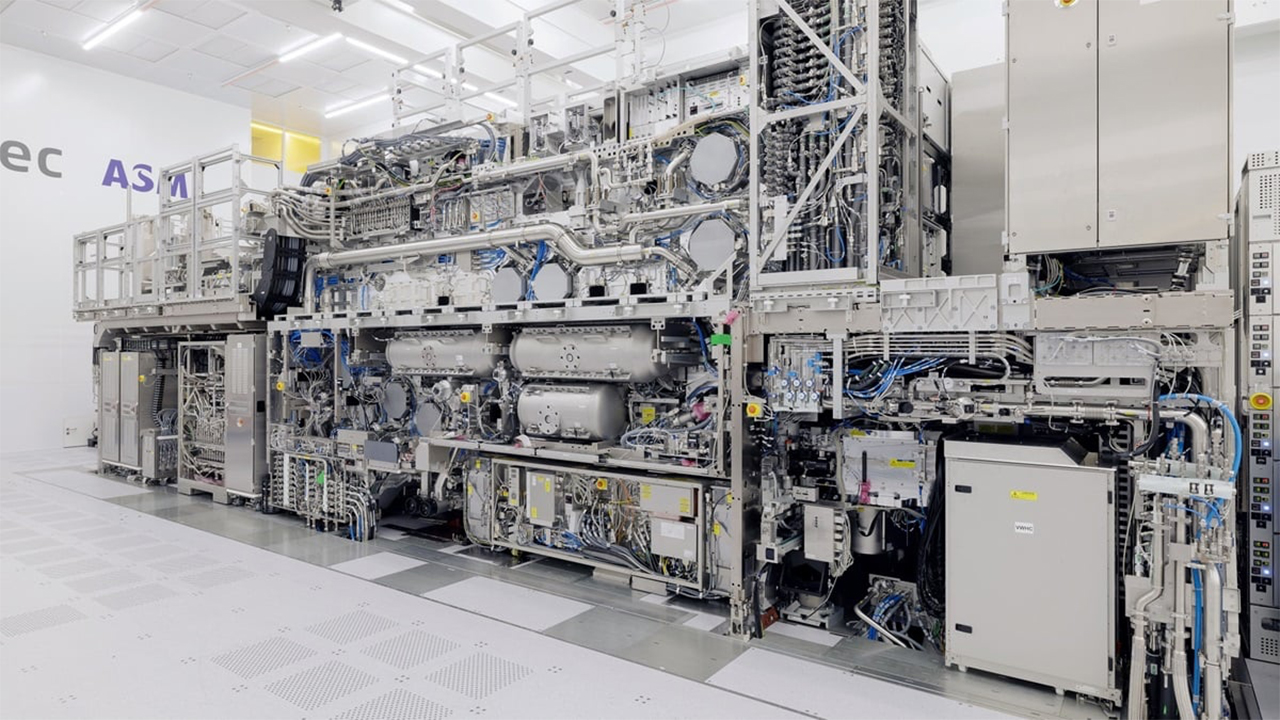
When Dutch officials revoked ASML’s license to export Twinscan NXT:2050i and NXT:2100i extreme ultraviolet (EUV) lithography systems to China under U.S. pressure, it closed the door to the only machines capable of producing sub-7nm chips at scale.
That single policy decision has defined what some analysts are calling the semiconductor cold war, where SMIC and its peers cannot buy the equipment needed for modern AI accelerators, and every shipment of advanced tools is now scrutinized as if it were a weapons transfer.
Sanctions and the scramble for workarounds
EUV machines are some of the most complex industrial systems in existence. Packed with thousands of U.S.-origin components and priced at hundreds of millions of dollars a piece, they are the foundation of every 5nm and 3nm chip shipping, or planning to ship in the future. China has none, and the U.S. has made sure of that.
Successive rounds of sanctions since 2022 have blocked not just EUV exports, but also the most advanced immersion DUV systems, including ASML’s Twinscan NXT:1970i and NXT:1980i. The Netherlands and Japan joined those restrictions, and even service contracts for ASML machines installed in China are being scrutinized. ASML itself has admitted that a China-based employee stole proprietary EUV data, highlighting how valuable the technology has become.
The policy has pushed chip procurement into murky territory. Grey-market Nvidia GPUs continue to flood in through Hong Kong and Singapore despite being explicitly banned, with seizures measured in the hundreds of millions of dollars. But smuggling a workstation card is one thing; sneaking in a 180-ton lithography scanner is another. On that front, Washington’s chokehold on export controls has held up.
The DUV fallback plan
Deep ultraviolet lithography predates EUV by decades. Using 193nm argon-fluoride lasers, immersion DUV systems comfortably support 28nm nodes, with yields and costs increasing dramatically as nodes shrink further. With multi-patterning (exposing the same wafer multiple times with different masks) they can be stretched down to 7nm-class geometries. Intel’s disastrous 10nm rollout proved how costly and yield-sensitive that approach can be, but it remains the only path available to Chinese fabs.
SMIC’s Kirin 9000-class parts, built for Huawei, already demonstrate the limits of this strategy. It’s widely believed that they were fabricated with DUV and heavy use of multiple patterning. The chips work, but at lower volume and efficiency than anything coming out of Taiwan or South Korea.
For now, Chinese fabs are leaning on their existing ASML DUV fleets. Nearly half of ASML’s second-quarter equipment tooling shipments in 2024 went to China, despite the political pressure in Washington. Those sales are a reminder of just how dependent Beijing still is on imported tools. But the window is closing, and the focus is shifting.
Shanghai Micro Electronics Equipment announced in 2023 that it had built a 28nm immersion scanner, the SSA800-10W. It’s crude compared to ASML’s Twinscan line, but it represents the first domestically developed immersion tool, and critically, it was designed without U.S. intellectual property. According to a TrendForce report, SMIC is testing a prototype from Yuliangsheng, a Huawei-linked affiliate of SiCarrier, which also rated for 28nm, but with ambitions to scale toward 7nm with multi-patterning.
A fully domestic DUV scanner, even if mired in yield problems, would insulate Chinese foundries from future Western policy decisions. Let’s not forget that China has previously made it clear that strategic self-sufficiency matters more than perfect parity with TSMC or Samsung.
China is playing the long game
Nobody expects China’s DUV tools to rival ASML’s. The gap is at least a decade, and without EUV, the economics are punishing. Multi-patterning consumes more wafers, introduces more points of failure, and demands ever more sophisticated etch and metrology equipment to hold yields together. Every advanced chip that comes off a DUV line in Shanghai costs more than its equivalent in Hsinchu.
Even with low yields, however, a 7nm-class domestic chip is better than none at all. Huawei has already rebuilt much of its smartphone supply chain around local vendors, and state mandates now require Chinese firms to source 50% of their chips domestically.
Meanwhile, ASML’s chief executive has said China is ten to fifteen years behind. That may be true in technology, but sanctions are accelerating the drive to close the gap. Each ban entrenches the incentive to localize, and each domestic stepper tested at SMIC or Huawei’s labs makes the next round of controls less decisive.
That is the paradox of the so-called semiconductor cold war. EUV has been locked down, but in the process, DUV has become the backbone of a new, homegrown ecosystem. For Washington, the risk is that every workaround makes China a little less dependent. And for China, the bet is that a decade of inefficiency is worth the price of eventual independence.
Follow Tom's Hardware on Google News, or add us as a preferred source, to get our up-to-date news, analysis, and reviews in your feeds. Make sure to click the Follow button!


 English (US) ·