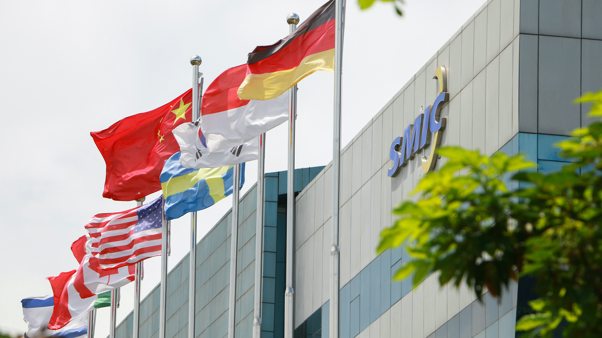
SMIC, the largest foundry in China, is test-driving one of China's first domestic immersion DUV lithography tools, reports Financial Times. The system was developed by Shanghai Yuliangsheng Technology Co., which is linked to Huawei's SiCarrier, and is believed to be a significant part of China's effort to become self-sufficient in wafer fab equipment.
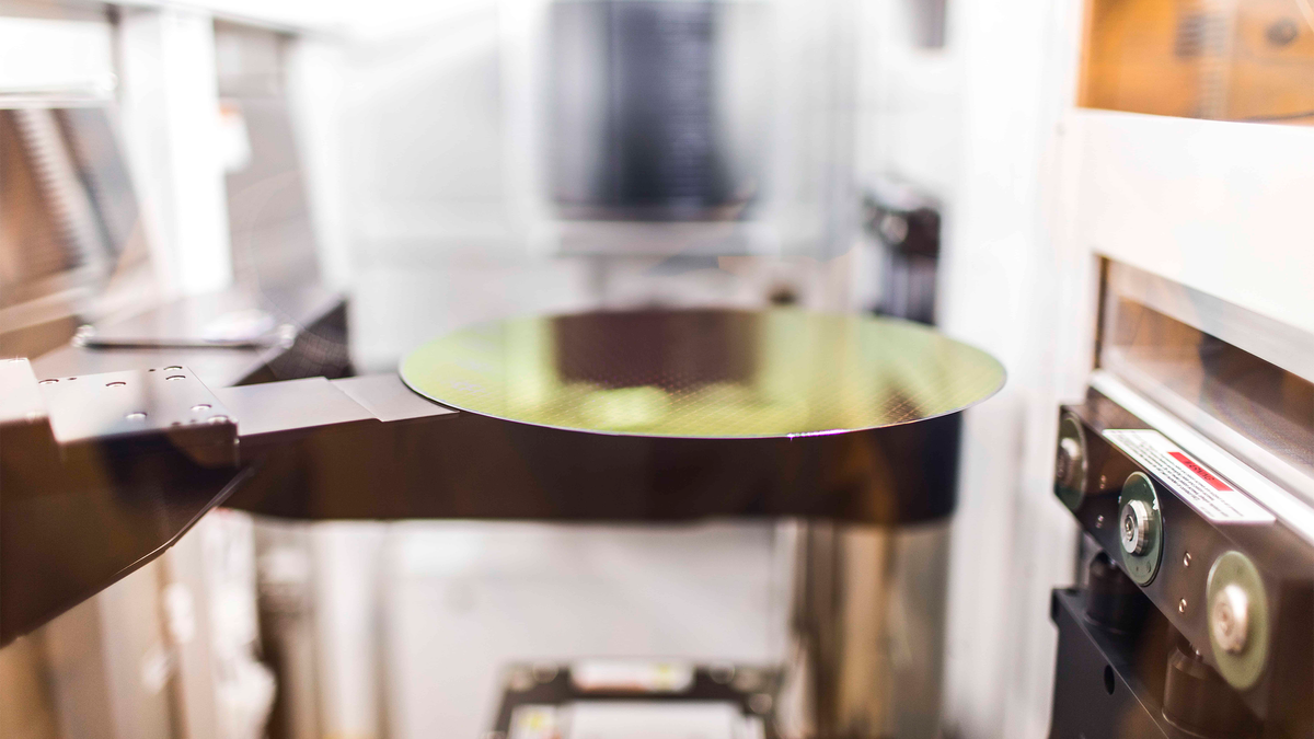
SMIC's test platform from Yuliangsheng involves a DUV machine that uses immersion lithography and is reportedly designed for 28nm-class fabrication technologies, though it could be used for 7nm or even 5nm production nodes by applying multipatterning. The Yuliangsheng tool is mostly made from components sourced within China, although some parts are still imported. The company is actively working to localize the entire supply chain. Once that is achieved (though it is unclear when), it would allow China to operate outside the influence of the U.S. or European export policies in this segment of chip production.
If the description of the tool by Financial Times is accurate, then the Yuliangsheng immersion DUV system currently being tested by SMIC resembles ASML's Twinscan NXT:1950i from 2008, which was designed for 32nm-class process technology in one exposure. The unit featured optics with 1.35 numerical aperture, a 2.5nm overlay, a 38nm resolution, and could be used for making chips on a 22nm-class fabrication node. While theoretically the NXT:1950i could be used to make chips on 7nm and 5nm-class nodes, ASML has developed NXT:2000i for such fabrication technologies, which is generations ahead of the NXT:1950i.
It is unclear whether the Yuliangsheng tool is being tested within SMIC's production flow (i.e., they are producing actual chips or patterns) or if the company is just beginning to test the scanner and has merely reached first light on the wafer or first patterning milestones (a more likely scenario). If it is the latter, then the scanner is years away from mass-producing actual chips. Indeed, the goal is reportedly to integrate domestic immersion DUV lithography machines into production lines starting in 2027, after their qualification. Before that, SMIC will continue to rely on tools from ASML.
It should be noted that while SMIC (and probably Yuliangsheng) believes that it is possible to build chips on 7nm and 5nm-class process technologies on the same tools that are used for 28nm-class production nodes, it remains to be seen whether this is possible without a dramatic improvement of a 28nm-class tool when it comes to overlay performance, precision, control, and complexity. Essentially, after the existing tool matures and gets inserted into SMIC's 28nm flow in 2027, it will take Yuliangsheng years to jump to 16nm and then to 7nm fabrication nodes with a significantly redesigned scanner, so do not expect SMIC's sub-10nm fabrication processes on domestic lithography systems earlier than in 2030.
The tool is codenamed 'Mount Everest,' after the world's tallest mountain, perhaps highlighting the importance of the project. Interestingly, but SiCarrier also tends to call its WFE projects after mountains, which perhaps proves that SiCarrier and Shanghai Yuliangsheng Technology Co. are not only affiliated (SiCarrier is reportedly an investor of Yuliangsheng), but likely belong to the same group working on the same goal. It is noteworthy that Shanghai Yuliangsheng Technology Co. is already known to the U.S. Department of Commerce, which put it into its Entity List in late 2024.
Follow Tom's Hardware on Google News, or add us as a preferred source, to get our up-to-date news, analysis, and reviews in your feeds. Make sure to click the Follow button!
Get Tom's Hardware's best news and in-depth reviews, straight to your inbox.
 1 month ago
18
1 month ago
18


 English (US) ·