 6 months ago
19
6 months ago
19
While many fabs co-funded by the U.S. government under the CHIPS and Science Act are being built or are about to start ramping production of semiconductors, there are some facilities for which construction has not started due to environmental reviews and protests of local residents, with companies "mired in NIMBY fights and two-year permits." Among such projects are Amkor's advanced packaging facility in Arizona, Micron's DRAM fab in New York, and SK hynix's HBM facility in Indiana, reports SemiAnalysis.
Locals oppose Amkor's facility
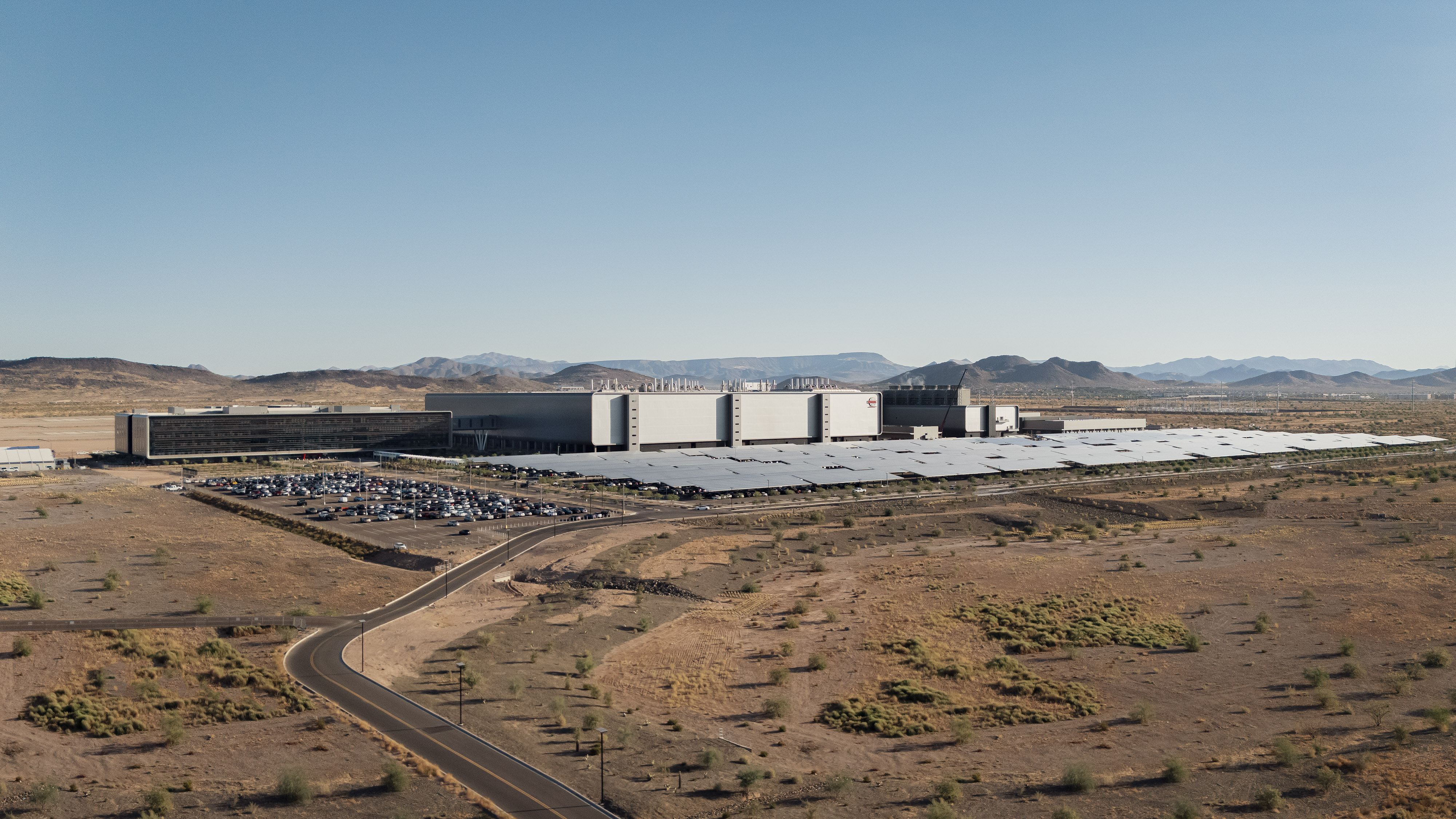
Amkor's plan to build a $2 billion chip packaging facility near Peoria, Arizona, is facing resistance from nearby residents of Vistancia. The locals are opposing Amkor's proposed site due to concerns about the potential strain on water resources and increased traffic congestion. Some residents are threatening legal action and calling for the project to be moved elsewhere.
Amkor's advanced packaging facility, which will include over 500,000 square feet (46,451 square meters) of cleanroom space when constructed and equipped, is crucial for the local semiconductor supply chain that already includes TSMC's Fab 21 campus as well as over a dozen suppliers. The plant, which is expected to be one of the world's largest advanced packaging factories in the world, is also crucial for companies like Apple, which has committed to building chips at TSMC's Fab 21 and packaging them at Amkor's facility. However, given the ongoing protests, it remains to be seen whether the plant will come online in 2027, as planned.
Micron's $100 billion campus faces delays
The situation is not unique to Amkor and Arizona. In Clay, New York, Micron's planned massive $100 billion DRAM production site (originally expected to be completed in the 2040s and create some 50,000 direct and indirect jobs) has experienced scheduling setbacks. The company's environmental review was delayed, and the period for public feedback has been extended through August. As a result, construction, which was supposed to start in 2024, cannot begin until community objections are resolved.
The campus near Clay, New York, was expected to become the largest manufacturing site Micron has ever developed and one of the biggest semiconductor facilities in the United States. The site is projected to house four clean rooms totaling 600,000 square feet (around 55,700 square meters), which is about eight times larger than the clean room space at GlobalFoundries' Fab 8 facility.
The fab is a key part of Micron's strategy to expand its U.S. production. The initial stage of construction in Clay was projected to require approximately $20 billion in spending through the end of this decade, setting the stage for the larger buildout planned in the following years. However, Micron is facing massive delays, so instead of earning a million a day later this decade producing memory in the U.S., the company will have to invent ways to produce enough DRAM later in the 2020s. According to the report, delays on a $20B fab are costing $5M per day.
Micron planned to manufacture 40% of its DRAM output within the United States by the mid-2030s, operating its facilities near Boise, Idaho, and Clay, New York. However, given the current delay, it is unclear whether Micron manages to execute its plan.
SK hynix gets approval, but that was hard
In West Lafayette, Indiana, SK hynix obtained approval for its $3.9 billion high-bandwidth memory (HBM) production site, but it took it seven hours to persuade the city council. The company faced resistance from local residents regarding the rezoning of over 120 acres near their homes. Residents expressed concerns about industrial development near residential zones, nearly stalling the project.
The $3.9 billion facility dedicated to HBM and other exotic types of memory is expected to be one of the biggest and most sophisticated DRAM assembly facilities on the planet when it starts operations in 2028. The plant is projected to create up to 1,000 jobs, and SK hynix also plans to partner with Purdue University over future R&D projects.
Preventing delays
To prevent such delays in future developments, some states are creating pre-approved industrial locations, according to SemiAnalysis. North Carolina, Pennsylvania, and Ohio have funded large-scale sites equipped with utilities and baseline environmental clearance. These areas are designed to host manufacturing operations without extended permitting procedures, making them more attractive to semiconductor firms.
Supporters of this strategy argue that early-stage preparation reduces costs, simplifies compliance, and accelerates supplier commitments. By planning infrastructure in advance, states can also impose penalties if promised investments fall through, ensuring greater accountability from companies.
Streamlining approval processes has become a competitive advantage in global technology development. According to analysis from the Center for Security and Emerging Technology, the speed at which facilities can be permitted is now a critical factor in determining the pace of semiconductor manufacturing expansion and attractiveness of countries for large chipmakers.
Follow Tom's Hardware on Google News to get our up-to-date news, analysis, and reviews in your feeds. Make sure to click the Follow button.


 English (US) ·