 1 day ago
16
1 day ago
16
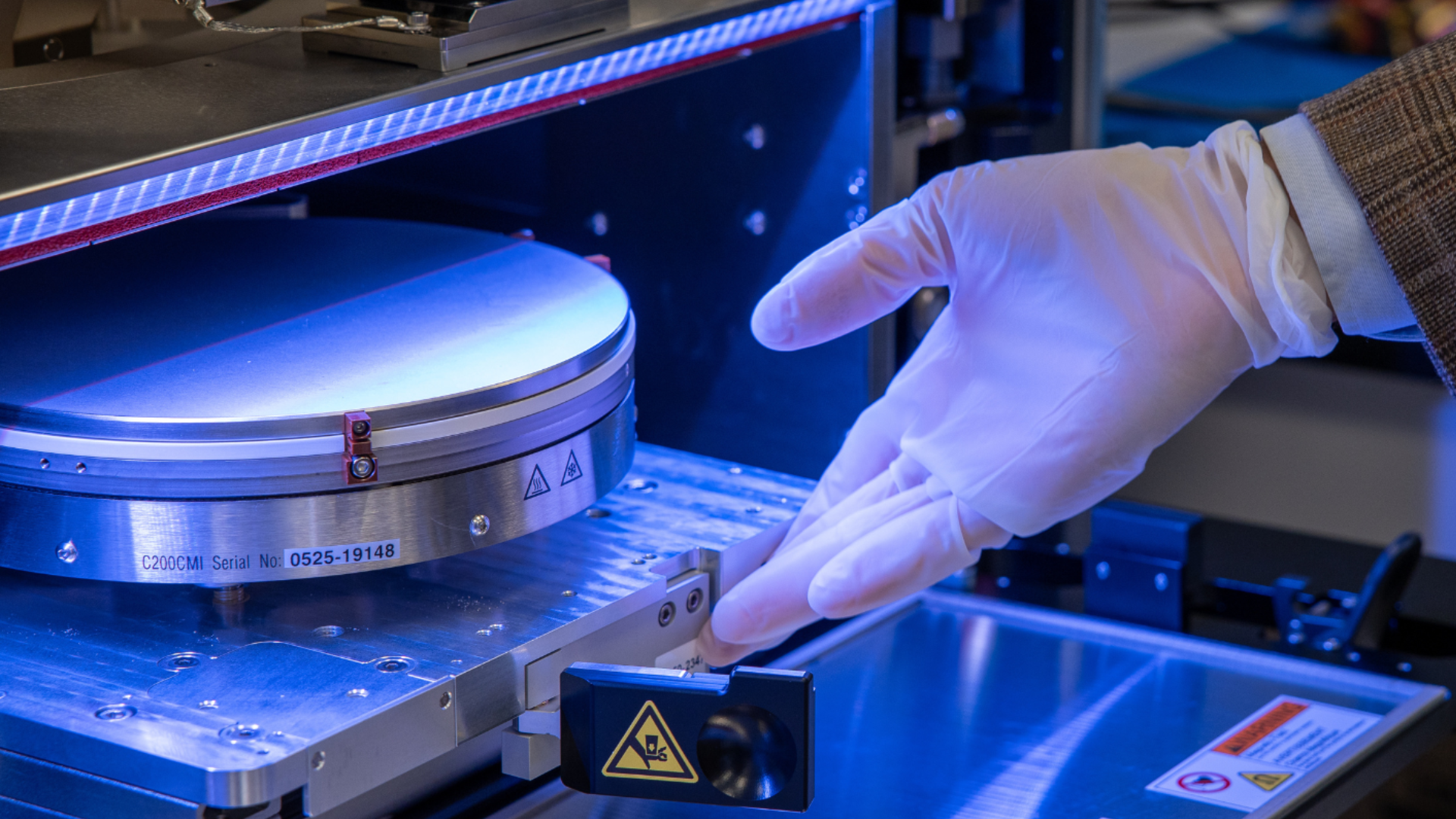
A collaborative research team has demonstrated what it says is the first monolithic 3D integrated circuit manufactured at a commercial U.S. foundry, reporting substantial performance gains over conventional flat chip designs. The prototype was developed by engineers from Stanford, Carnegie Mellon, the University of Pennsylvania, and MIT, and fabricated in partnership with SkyWater Technology.
The chip departs from conventional two-dimensional layouts by stacking memory and logic directly on top of one another in a single, continuous process. Instead of assembling multiple finished dies into a package, the researchers built each device layer sequentially on the same wafer using a low-temperature process designed not to damage underlying circuitry, resulting in a dense network of vertical interconnects that shortens data paths between memory cells and compute units.
Twelve-fold performance improvements seen in simulations
Beyond the measured hardware results, the researchers also evaluated taller stacks through simulation. Designs with additional tiers of memory and compute showed up to a twelve-fold performance improvement on AI-style workloads, including models derived from Meta’s LLaMA architecture. The group further argues that the architecture could eventually deliver 100-fold to 1,000-fold improvements in energy-delay product, a combined metric of speed and efficiency, by continuing to scale vertical integration rather than shrinking transistors.
While academic labs have previously demonstrated experimental 3D chips, the team emphasizes that this work differs in being built in a commercial foundry environment rather than a bespoke research line. SkyWater executives involved in the project described the effort as proof that monolithic 3D architectures can be transferred into domestic manufacturing flows, rather than remaining confined to university cleanrooms.
"Turning a cutting-edge academic concept into something a commercial fab can build is an enormous challenge," said co-author Mark Nelson, vice president of technology development operations at SkyWater Technology.
The team presented their research at the IEEE International Electron Devices Meeting (IEDM 2025) between December 6 and 10.

Follow Tom's Hardware on Google News, or add us as a preferred source, to get our latest news, analysis, & reviews in your feeds.


 English (US) ·