 8 months ago
20
8 months ago
20
Intel is set to detail (PDF) the advantages of its 18A manufacturing technology (1.8nm-class) compared to its Intel 3 fabrication process at the upcoming VLSI Symposium 2025. As expected, the new production node will offer substantial benefits across power, performance, and area (PPA) metrics, thus providing tangible advantages both for client and data center products.
Intel claims that its 18A fabrication process delivers 25% more performance at the same voltage (1.1V) and complexity, as well as 36% lower power at the same frequency and voltage of 1.1V for a standard Arm core sub-block compared to the same block fabricated on Intel 3 process technology. At a lower voltage (0.75V), Intel 18A provides 18% higher performance and 38% lower power. In addition, 18A consistently achieves 0.72X area scaling compared to Intel 3.
Intel's 18A manufacturing technology is the company's first node to rely on gate-all-around (GAA) RibbonFET transistors and feature PowerVia backside power delivery network (BSPDN), two features that enable major PPA advantages.
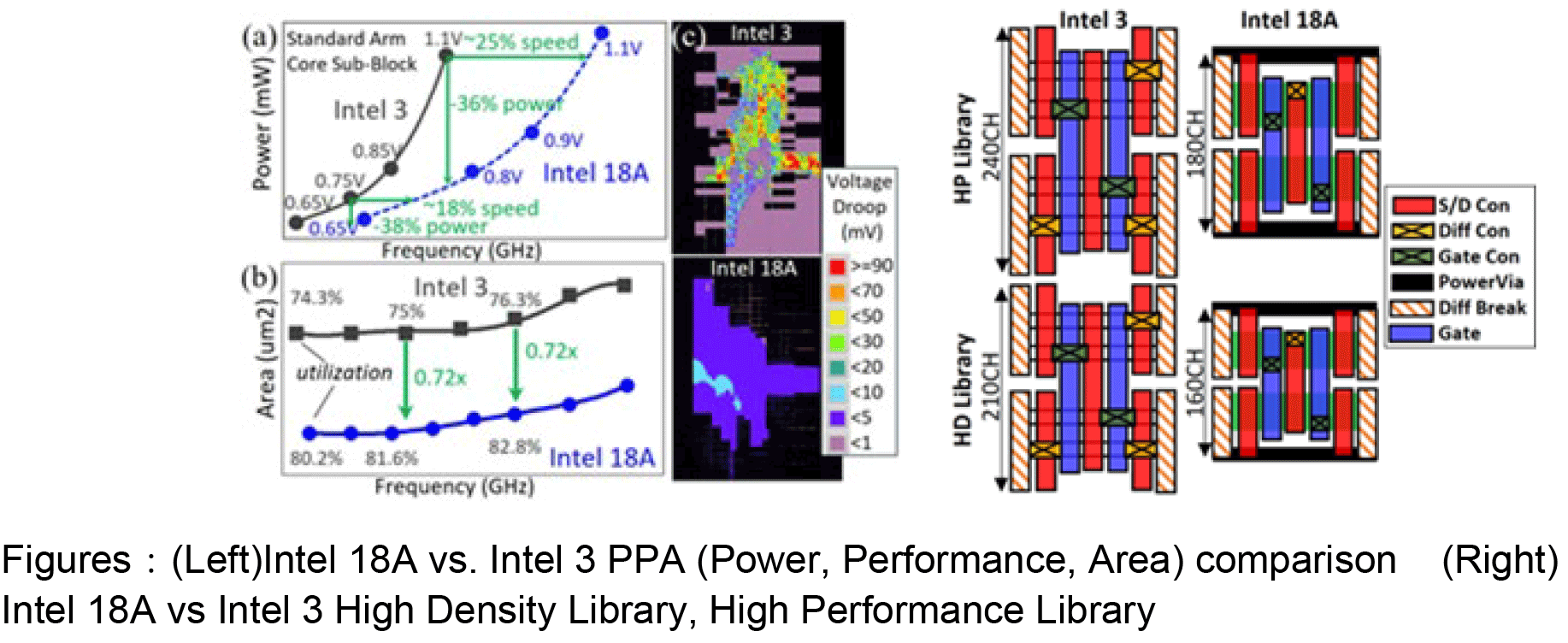
The standard cell layout comparison highlights the significant physical scaling achieved by Intel 18A over Intel 3 in both High-Performance (HP) and High-Density (HD) libraries. Intel 18A reduces cell heights from 240CH to 180CH in HP libraries and from 210CH to 160CH in HD libraries, which represents a ~25% reduction in vertical dimension. This tighter cell architecture allows for increased transistor density, contributing directly to improved area efficiency.
The use of PowerVia BSPDN enables more efficient vertical routing by offloading power lines from the front side of ICs, freeing up space for signal routing and further compacting the layout. Additionally, refined gate, source/drain, and contact structures improve overall cell uniformity and integration density. These enhancements collectively enable Intel 18A to deliver better performance-per-area and energy efficiency, supporting more advanced and compact chip designs.
Intel is reportedly on track to start high-volume manufacturing of compute chiplets for its codenamed Panther Lake processors for client PCs later this year and then chiplets for Clearwater Forest data center systems in early 2026. In addition, the company is on track to tape out the first third-party designs on 18A in mid-2025.
Apparently, there is interest in developing third-party chips for Intel 18A. In addition to presenting a general paper describing its 18A technology, Intel plans to present a paper describing a PAM-4 transmitter implemented using 18A production node with a BSPDN that is co-authored by engineers from Intel, Alphawave Semi (a contract chip designer and IP provider), Apple, and Nvidia. This does not necessarily mean that Apple or Nvidia will use Intel's 18A for production silicon, but this at least means that they are interested in checking it out.
Speaking of Apple and Nvidia, TSMC said that virtually all of its partners plan to adopt its N2 (2nm-class) process technology, so it is reasonable to expect this node to be more widely used than Intel's 18A. Nonetheless, for Intel it is crucial to show that it can develop a competitive node and ramp it to high volume, so 18A will play a vital role for the future of Intel's foundry business.


 English (US) ·