 7 months ago
38
7 months ago
38
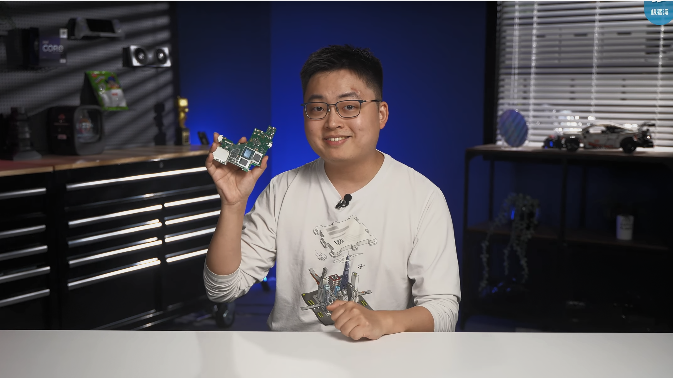
While we still have a month before the Nintendo Switch 2 makes its official debut, hardware sleuth Geekerwan managed to obtain an engineering board for the device. This allowed him to put the onboard Tegra T239 SoC under a FIB-SEM (Focused Ion Beam Scanning Electron Microscope) to examine the chip's internals, allowing for precise layer-by-layer analysis of the structure, revealing important details such as the core layout and process node.
Given Nintendo's strict legal stance and letigous precedents, it's quite amazing how Geekerwan managed to get ahold of the board, proceeded to dissect the SoC, and spilled all the juicy details on YouTube. Apparently, the board was acquired by hardware analyst Kurnal from Xianyu (Taobao's version of eBay) and then passed on to Geekerwan. Either way, this analysis answers many questions, as Nintendo has yet to officially disclose many SoC details.
The Switch 2 SoC measures around 207mm2 in size, twice as large as the previous X1 SoC (Mariko/Tegra T210). This exact unit was taped out sometime in 2021, and is codenamed "Tegra T239" as revealed by the stamps on the metal layers of the chip after decapping. This suggests the Switch 2 was planned for an earlier reveal, but was likely postponed due to unknown reasons.
Based on the data gathered by Geekerwan, the Switch 2's SoC uses a customized Samsung process that blends features from its 10nm and 8nm technologies. In essence, it carries similar characteristics to Samsung's 8N node employed on the RTX 30 series, but is slightly different. Earlier speculation suggested Nintendo might employ a more advanced 5nm process. However, porting Ampere, which was originally designed for 8N, to a completely new process would necessitate redesigning and revalidating all IP blocks, with added costs, and that's something Nintendo likely wanted to avoid.
This is Nintendo Switch 2's CPU! - YouTube
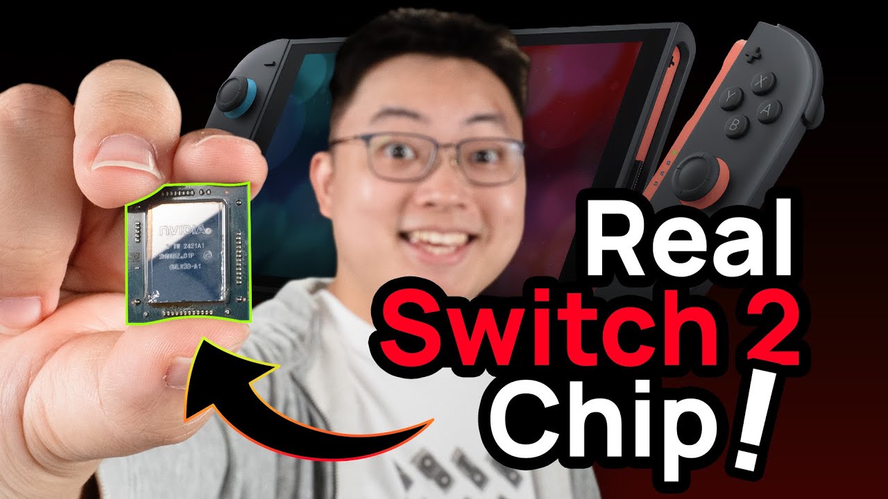
The closest relative to the T239 is Nvidia's Tegra T234 used in the Jetson Orin. Die-shot analysis of the T239 reveals 8x Arm Cortex-A78C cores, each with 256KB of private L2 cache, sharing a 4MB L3 pool, next to an Ampere-based GPU, likely based on the GA10B die, with 6 TPCs, for a total of 12 SMs or 1,536 Ampere-based CUDA cores. The CPU-side A78AE (T234) and A78C (T239) cores are similar in size at 2.4mm2, however, each GPU SM (Streaming Multiprocessor) in the T239 (2.71mm2) is 22% smaller than the T234 (3.47mm2). Interestingly, both of these carry larger SMs than the GA102-based RTX 3090, which sits at 2.57mm2.
Aside from the SoC, the board is equipped with 256GB of TLC-based UFS 3.1 storage from SK hynix, while the Wi-Fi and Bluetooth modules are sourced from MediaTek. The built-in power delivery system can supply up to 34.4W of power, though I doubt that the Switch 2 will actually need that much juice. Memory-wise, we're looking at 12GB (2x6GB) of LPDDR5x-8533 RAM from SK hynix. However, it'll likely be downclocked to 6400 MT/s (Docked) and 4266 MT/s (Handheld) to conserve power, like the previous Switch.
Geekerwan emulated the performance of the Switch 2 using an underclocked RTX 2050 laptop GPU. While not a one-to-one recreation, in synthetics, the laptop (using leaked docked specifications) showed similar performance to a GTX 1050 Ti, while the handheld-spec configuration matched a GTX 750 Ti, slightly inferior to the Steam Deck. We'll need to wait for the official embargo next month to get a better idea about the performance. However, it wouldn't be wrong to expect Nintendo to eye a mid-gen refresh using a more modern 5nm/3nm process.
Follow Tom's Hardware on Google News to get our up-to-date news, analysis, and reviews in your feeds. Make sure to click the Follow button.


 English (US) ·