 2 months ago
15
2 months ago
15
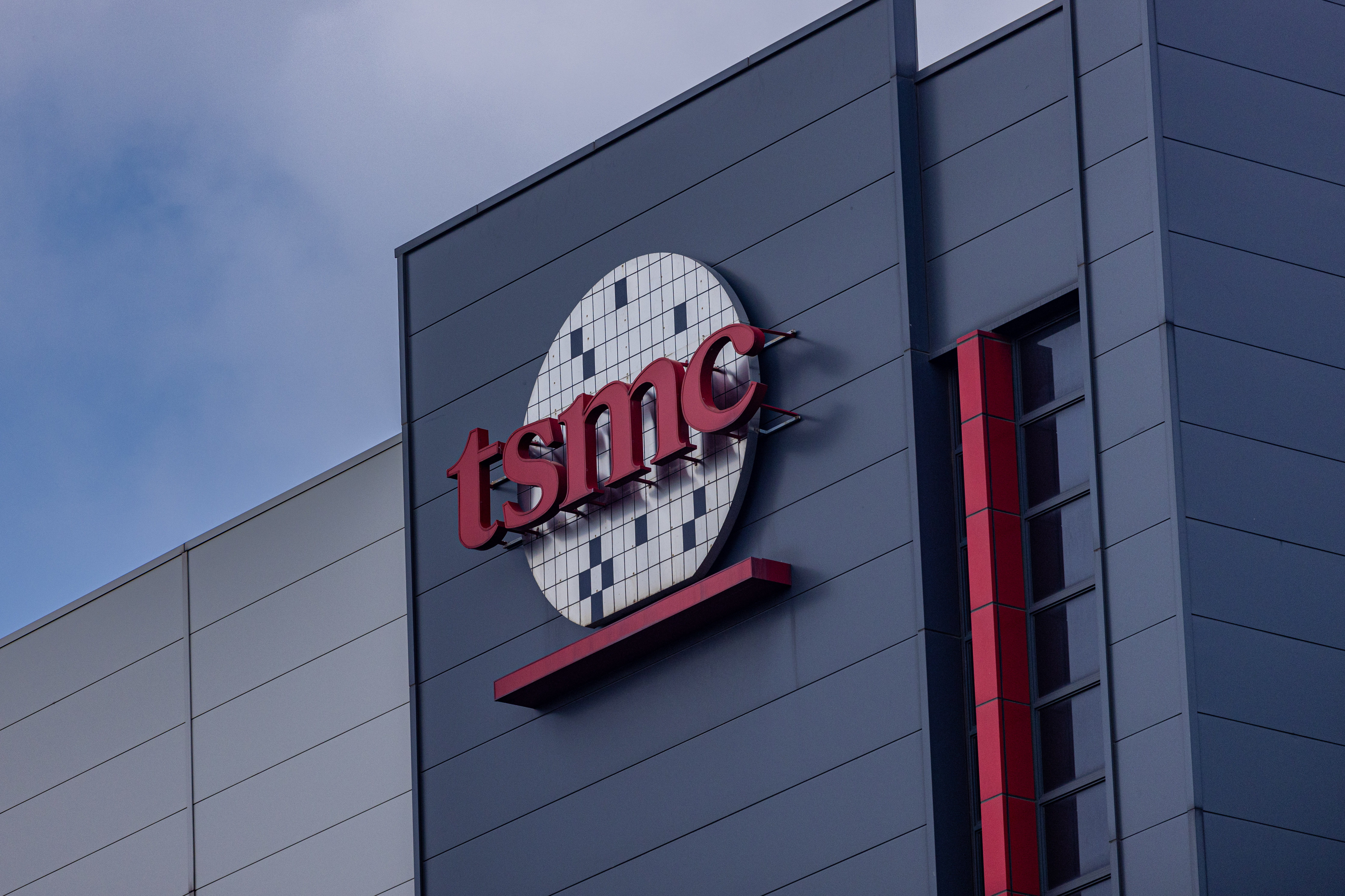
Nvidia will be the first customer to use TSMC’s A16 node, a 1.6nm-class process that marries gate-all-around (GAA) transistors with backside power delivery, according to China's Commercial Times. This is no small change in tradition: For more than a decade, Apple has been the one to break in each new process node from TSMC, with its iPhone SoCs serving as the high-volume anchor tenant.
But that tradition ends here. A16's first customer isn't building phones; its chips are designed for AI and other applications with extreme power delivery requirements. As TSMC’s first commercial node to integrate backside power delivery — which lifts power rails off the front and routes them through the back of the wafer — the foundry is pitching A16 as the natural progression from its N2 process.
What makes A16 different?
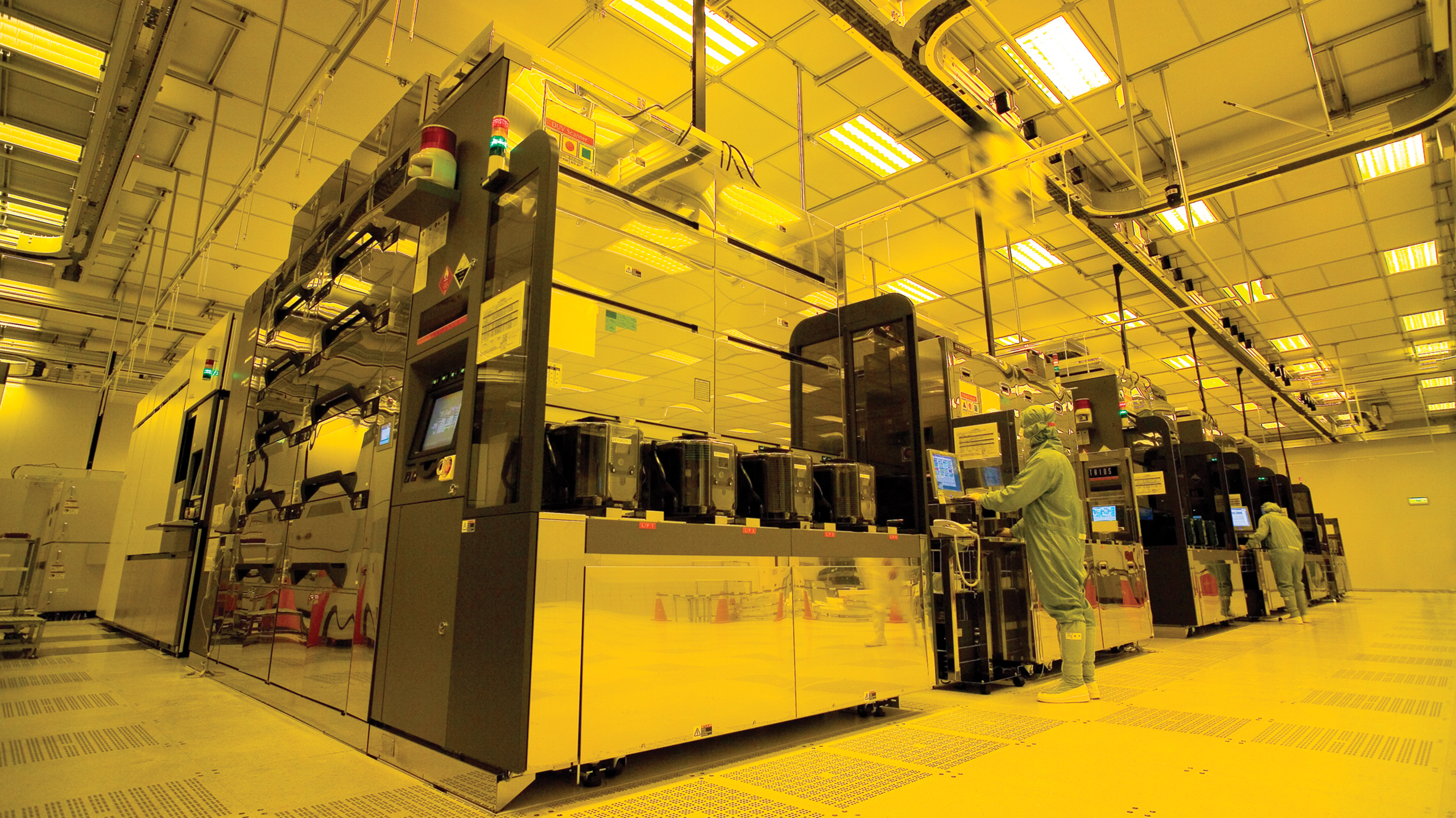
A16 is more than a shrink. It’s the first TSMC process to feature both GAA nanosheet transistors and backside power delivery. By shifting power delivery to the backside, signal routing on the front side becomes less constrained, reducing congestion and improving performance. Power reaches the transistors via a shorter, less resistive path, thereby reducing voltage drop and enabling higher frequencies or tighter integration.
TSMC claims that A16 delivers 8-10% higher speed or 15-20% lower power compared to baseline N2, plus a modest 7-10% density gain. The real benefit isn’t in the numbers, but rather what they unlock. With more available routing and cleaner power, large chips like GPUs gain new architectural freedom with wider cores, larger caches, more AI engines, and better scaling.
And because backside power delivery frees front-side metal for signals, it simplifies high-density hybrid bonding on the top surface. This makes 3D-stacked cache or vertically integrated SRAM more practical, and eases front-side congestion around wide I/O like HBM physical layers (PHYs), provided the design also employs fine-pitch hybrid bonding and adequate thermal mitigation at the package level.
The pressure is on
Nvidia’s decision to lead with A16 suggests that GPU designs are now pressing against front-side power delivery limits on advanced nodes. Moving power to the backside shortens the supply path and frees front-side interconnect, mitigating IR drop and routing congestion that become bottlenecks. In other words, these factors are turning backside power delivery into an architectural necessity for AI and HPC applications.
It also helps Nvidia leapfrog the competition. AMD is reportedly targeting standard 2nm for its next-gen EPYC and MI400-class accelerators. Intel’s 18A node is also expected to offer backside power through PowerVia around the same time. By moving straight to A16, Nvidia avoids this middle ground entirely and could potentially land with a full node advantage over its rivals with a chip based on Feynman architecture as early as 2028.
Naturally, gaining this edge won’t be cheap. Wafer pricing for A16 is rumored to exceed $30,000 based on N2 pricing, which far exceeds Apple’s typical wafer costs. But for Nvidia, where a single AI GPU can retail for tens of thousands, that premium might be easier to absorb. More importantly, Nvidia is betting that the node’s density and efficiency gains will more than offset the cost and lock in the company’s lead for the second half of the decade.
A calculated shift
Handing A16’s debut to Nvidia is a calculated shift for Nvidia. While Apple remains a major partner and is still expected to adopt baseline N2 for its 2026 iPhone 18 chips, Nvidia’s AI chips offer faster demand growth and a use case that showcases the A16’s strengths. AI chips are power hungry, bandwidth-constrained behemoths sensitive to layout limitations — and A16 has been built to address all these things.
It’s also not unthinkable to see this as a hedge against Intel. With its 18A process approaching, which also features a backside power solution, TSMC needs a flagship customer to prove it can execute at the same or higher level. Getting Feynman out the door on A16 before Intel gets any third-party 18A designs will help to reinforce TSMC’s leadership.
If Feynman on A16 is a success, it will ultimately set the tone for the next generation of AI silicon. Nvidia will have proven that backside power is not just viable but essential for extreme compute. That could force AMD, Intel, and others to accelerate their own roadmap decisions or risk falling behind on performance.
It may also reshape how packaging and architectures evolve. Designers will need new thermal models and power domain strategies to work with backside power delivery. Still, Nvidia’s status as the first to move in this territory will give it a leg-up in tooling and methodology — advantages that are difficult to copy.
Follow Tom's Hardware on Google News to get our up-to-date news, analysis, and reviews in your feeds. Make sure to click the Follow button.


 English (US) ·