Serving tech enthusiasts for over 25 years.
TechSpot means tech analysis and advice you can trust.
Forward-looking: Researchers at the University of Massachusetts Amherst have developed a laser-based technique to align 3D semiconductor chips, potentially overcoming a longstanding challenge in chip manufacturing. The method employs concentric metalenses to generate holograms that reveal misalignment between chip layers at a much smaller scale than previously possible.
Semiconductor chips have traditionally been manufactured in two dimensions. But as devices become more powerful and compact, the industry is increasingly turning to 3D chip designs, which involve stacking multiple 2D layers. This approach introduces significant technical challenges – most notably, the need to align each layer with extreme precision. Even slight misalignment can compromise chip performance.
The traditional approach for aligning two layers is to look with a microscope for marks, such as corners or crosshairs, on the two layers and to try to overlap them, said Amir Arbabi, associate professor of electrical and computer engineering at UMass Amherst and senior author of the study.
However, this microscope-based process is limited by the physical gap between layers and the need to refocus, which can actually cause the chips to shift and misalign further. The microscope cannot see both crosshairs in focus at once because the gap between the layers is hundreds of microns. The motion required to refocus between layers can lead to chip displacement, explained Maryam Ghahremani, the study's lead author.
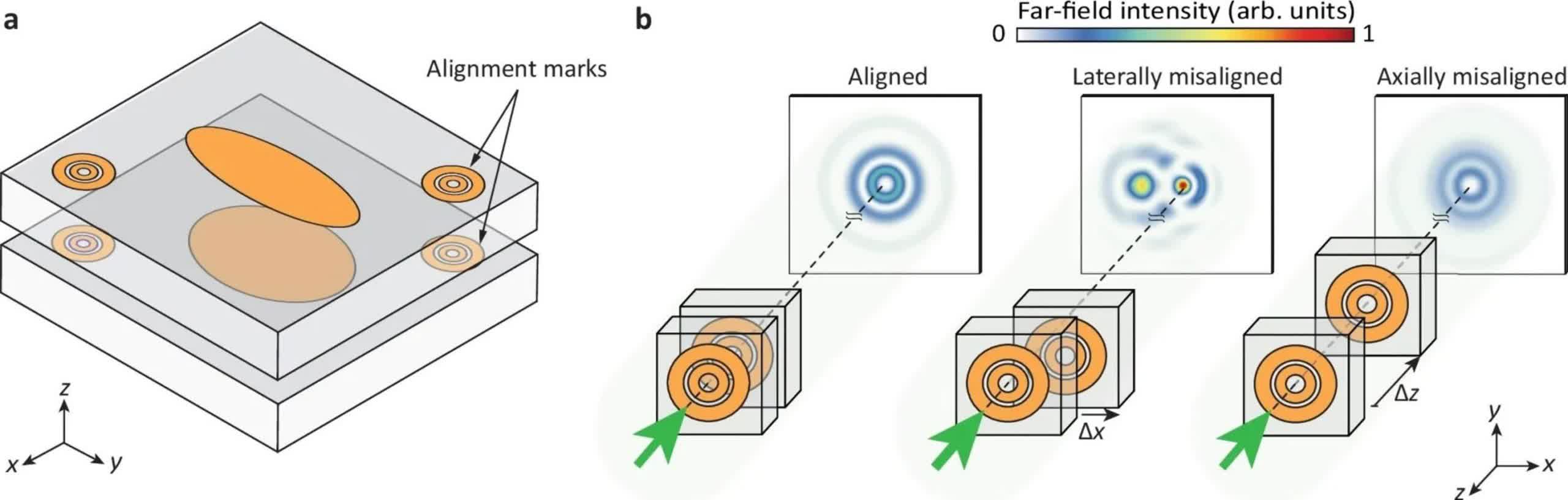
[Left] Semiconductor layers are stacked using concentric metalenses as alignment marks. [Right] Light shines through these marks to project a hologram. The alignment or misalignment of the lenses dictates the hologram's appearance.
Microscopes are also constrained by the diffraction limit, which restricts the smallest resolvable features to about 200 nanometers.
The new method developed at UMass Amherst bypasses these constraints. By embedding alignment marks made of concentric metalenses onto each chip and shining a laser through them, the researchers generate two interfering holograms. The resulting interference pattern provides a direct visual cue about the chips' alignment ,including both the direction and magnitude of any misalignment.
"This interference image shows if the chips are aligned or not, as well as the direction and the amount of their misalignment," Ghahremani said.
The system's precision exceeded initial expectations. While the team originally aimed for 100-nanometer accuracy, the method was able to detect misalignments as small as 0.017 nanometers along the horizontal axis and 0.134 nanometers along the vertical axis. "Consider you have two objects. By looking at the light that goes through them, we can see if one moved by the size of an atom with respect to the other one," Arbabi said.
This level of precision could have major implications for the semiconductor industry, where alignment errors remain a persistent and costly challenge. Reducing the technical and financial barriers to ultra-precise chip alignment could make advanced manufacturing more accessible to smaller companies and startups.
The researchers also suggest that the technique could be adapted for compact, low-cost sensors. "Many physical quantities that you want to detect can be translated to displacements, and the only thing you need is a simple laser and a camera," Arbabi said. Applications could include pressure sensors, vibration detectors, and other devices that monitor movement or environmental changes.


 English (US) ·