Serving tech enthusiasts for over 25 years.
TechSpot means tech analysis and advice you can trust.
In a nutshell: For more than half a century, the relentless progress of Moore's Law has driven engineers to double the number of transistors on a chip approximately every two years, fueling exponential growth in computing power. Yet as chips have become denser and more powerful, a formidable adversary has emerged: heat. Rising temperatures within modern CPUs and GPUs have far-reaching consequences that impact performance and power consumption. Over time, excessive heat slows critical signal propagation, degrades chip performance, and increases current leakage – wasting power and undermining the efficiency gains that Moore's Law once promised.
The underlying issue is closely linked to the end of Dennard scaling, a principle that once allowed engineers to shrink transistors and reduce voltage simultaneously – keeping power consumption in check. By the mid-2000s, however, further voltage reductions became impractical, even as transistor density continued to increase. This divergence led to a steady rise in power density and, inevitably, greater heat generation.
As chips grow more compact and powerful, managing thermal load has become a critical challenge for the semiconductor industry. According to James Myers, who leads the System Technology Co-Optimization program at Imec and authored a recent article for IEEE Spectrum, a new approach is needed to predict and address how evolving semiconductor technologies will influence heat generation and dissipation.
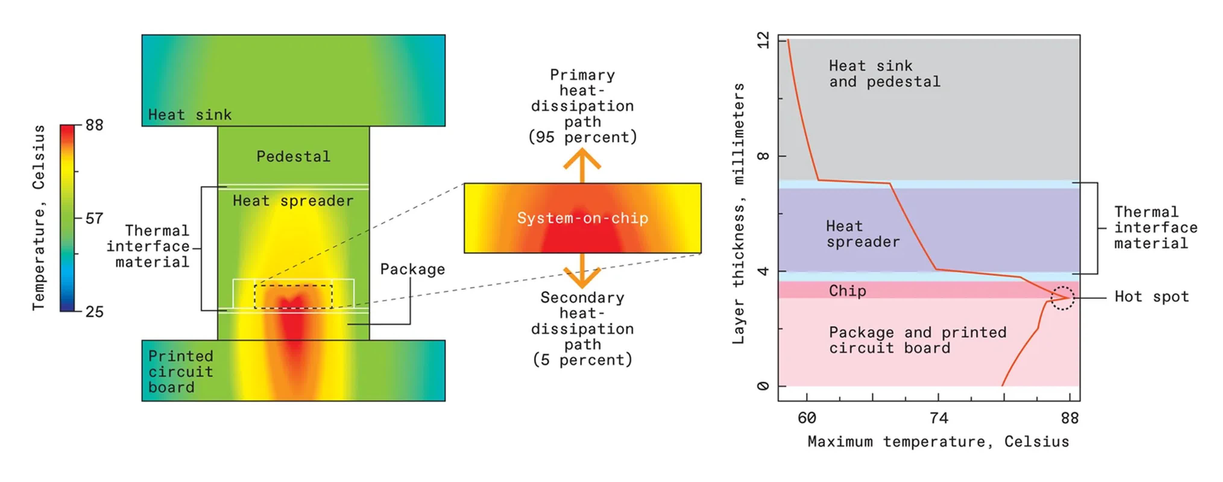
Heat follows a complex path as it's removed from a chip, but 95% of it exits through the heatsink.
Myers and his colleagues have developed a simulation framework that integrates industry-standard and open-source electronic design automation tools with proprietary software. This framework allows them to explore the interplay between chip technology and system-level thermal behavior.
Their findings are unequivocal: each new generation of semiconductor technology exacerbates the thermal challenge. Power density continues to rise as manufacturers transition to nanosheet transistors and, eventually, to complementary field-effect transistors (CFETs). Simulations of future technology nodes, such as A10 (1 nanometer) and A5, project a 12 to 15 percent increase in power density from A10 to A5, resulting in a temperature rise of approximately nine degrees Celsius at the same operating voltage.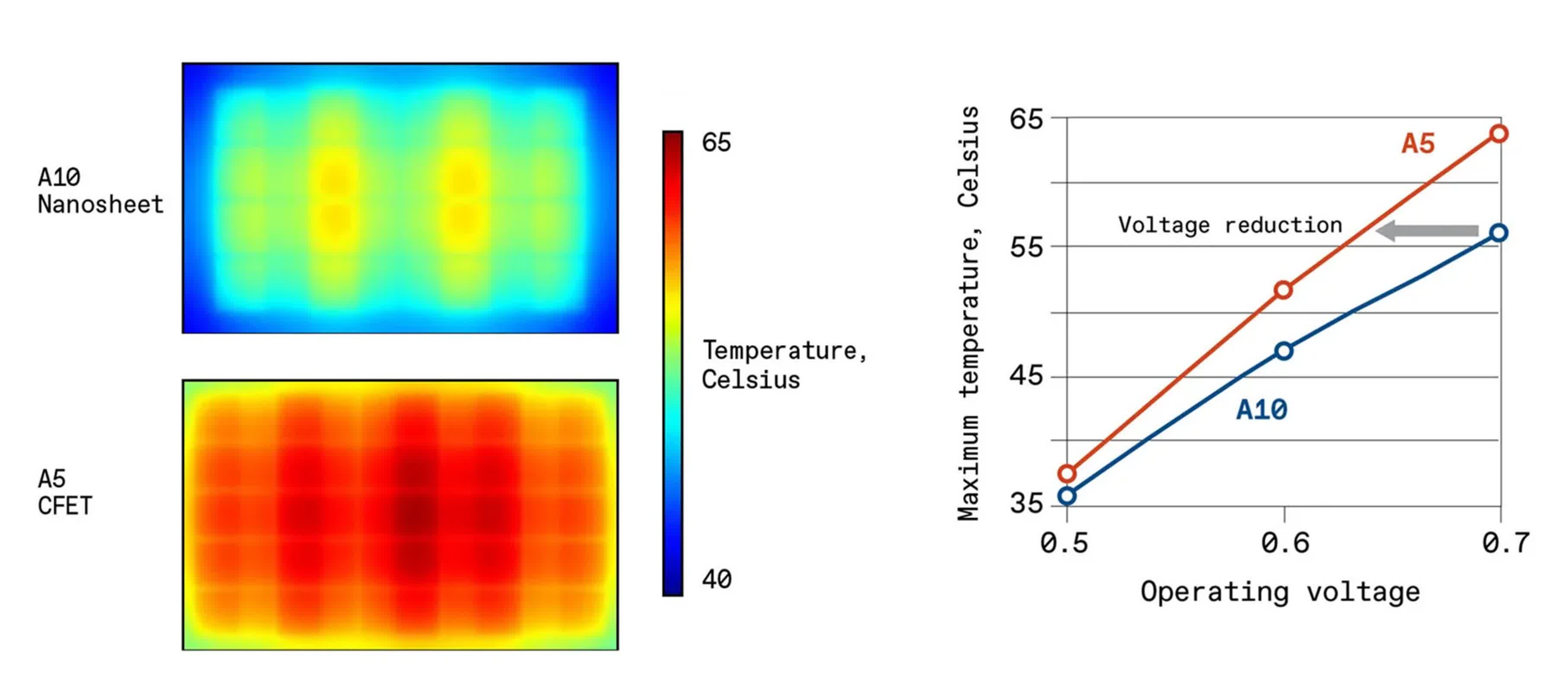
Complementary field-effect transistors will stack nanosheet transistors atop each other, increasing density and temperature. To operate at the same temperature as nanosheet transistors (A10 node), CFETs (A5 node) will have to run at a reduced voltage.
In data centers housing millions of chips, such an increase in power density could mark the difference between stable operation and catastrophic thermal runaway. Traditional cooling methods, such as air-cooled heatsinks, are already being supplemented by liquid cooling in high-performance facilities. However, even these advanced techniques may be insufficient to manage the heat generated by the next generation of chip technologies.
To address this, researchers are investigating alternative solutions, including microfluidic cooling, which channels coolant through microscopic passages embedded within the chip; jet impingement, which uses high-velocity coolant streams directed at the chip's surface; and immersion cooling, where entire boards are submerged in a thermally conductive dielectric fluid.
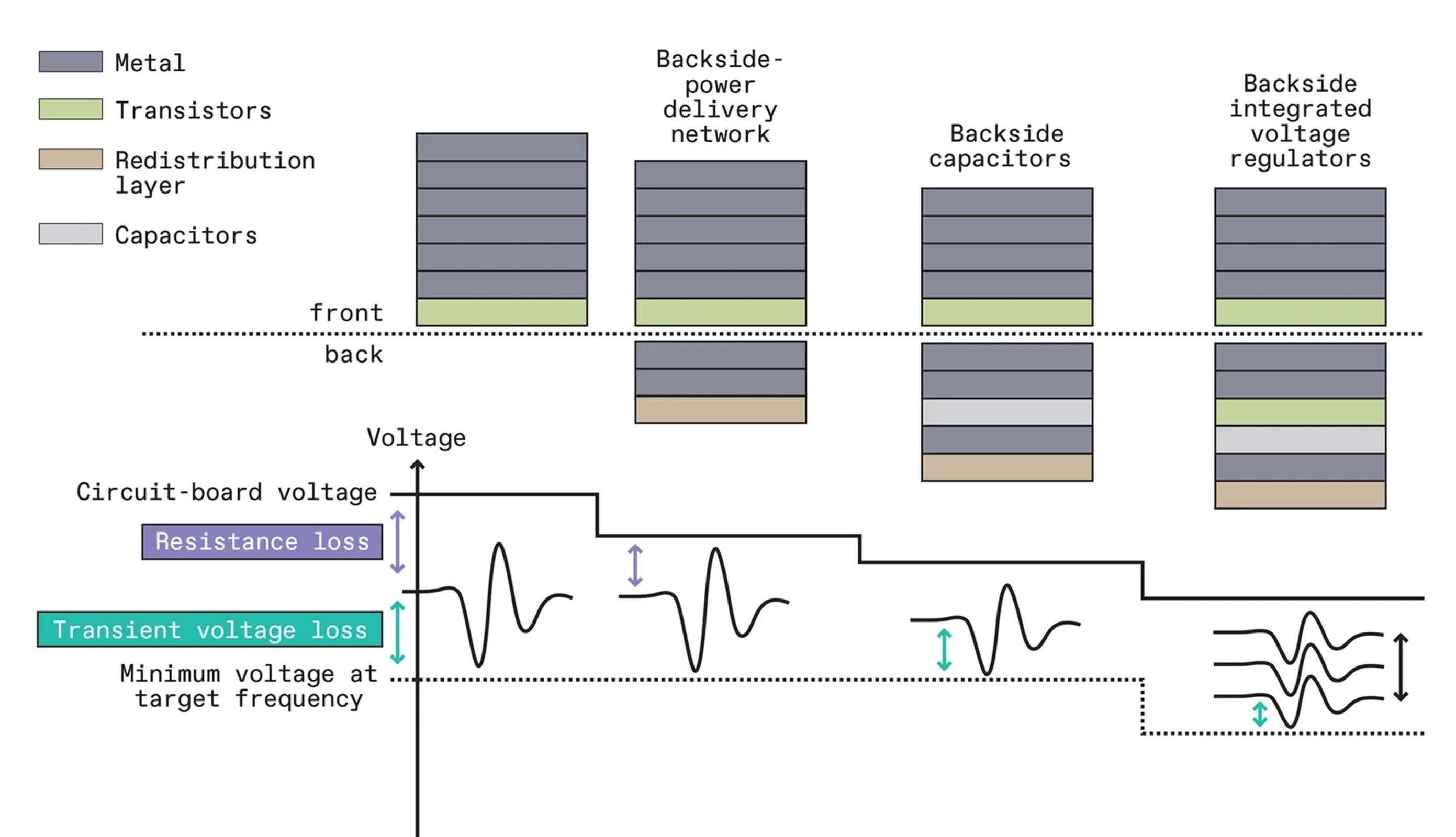
New technologies can reduce the voltage that needs to be delivered to a multicore processor so that the chip maintains a minimum voltage while operating at an acceptable frequency. A backside power-delivery network does this by reducing resistance. Backside capacitors lower transient voltage losses. Backside integrated voltage regulators allow different cores to operate at different minimum voltages as needed.
Yet these methods may not be practical in all settings – particularly in mobile devices where size, weight, and battery life are tightly constrained, or in data centers where infrastructure upgrades can be costly and disruptive.
Beyond cooling, system-level strategies are increasingly used to manage temperatures. Thermal sensors, for example, can trigger dynamic reductions in voltage and frequency to lower power consumption. However, this often comes at the expense of performance, a trade-off familiar to anyone whose smartphone slows down under the heat of direct sunlight.
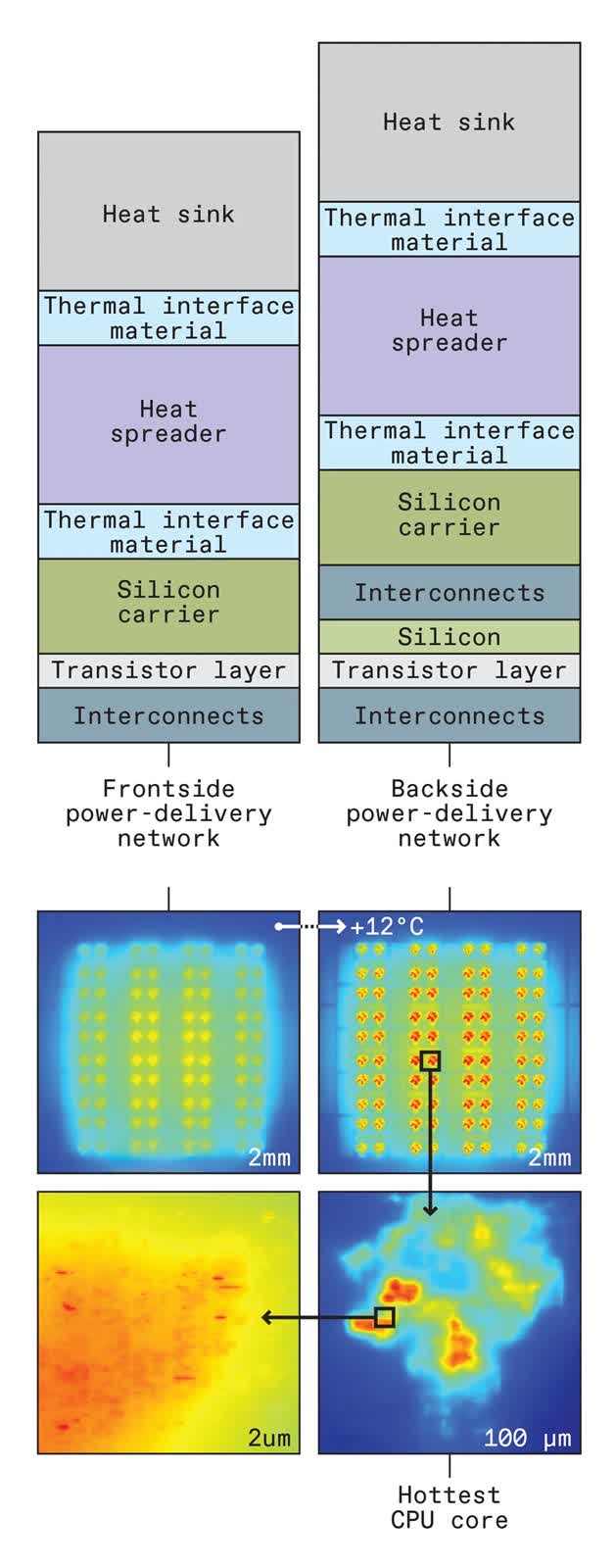
By changing the materials within the path of heat removal, backside power-delivery technology could make hot spots on chips even hotter.
Another technique, known as thermal sprinting, rotates workloads among processor cores, allowing overheated cores to cool while others take over. Although effective for short bursts of activity, this approach can reduce overall throughput and introduce latency during sustained workloads.
A promising new frontier in thermal management involves leveraging the backside of the chip wafer. By relocating the power delivery network to the underside of the chip, a strategy known as backside power delivery network (BSPDN), engineers can reduce electrical resistance and enable operation at lower voltages, thereby decreasing heat generation.
All major advanced CMOS foundries are expected to adopt BSPDN technology by 2026. Future enhancements may include integrating high-capacity capacitors and on-chip voltage regulators on the backside, enabling finer voltage control and further improving energy efficiency.
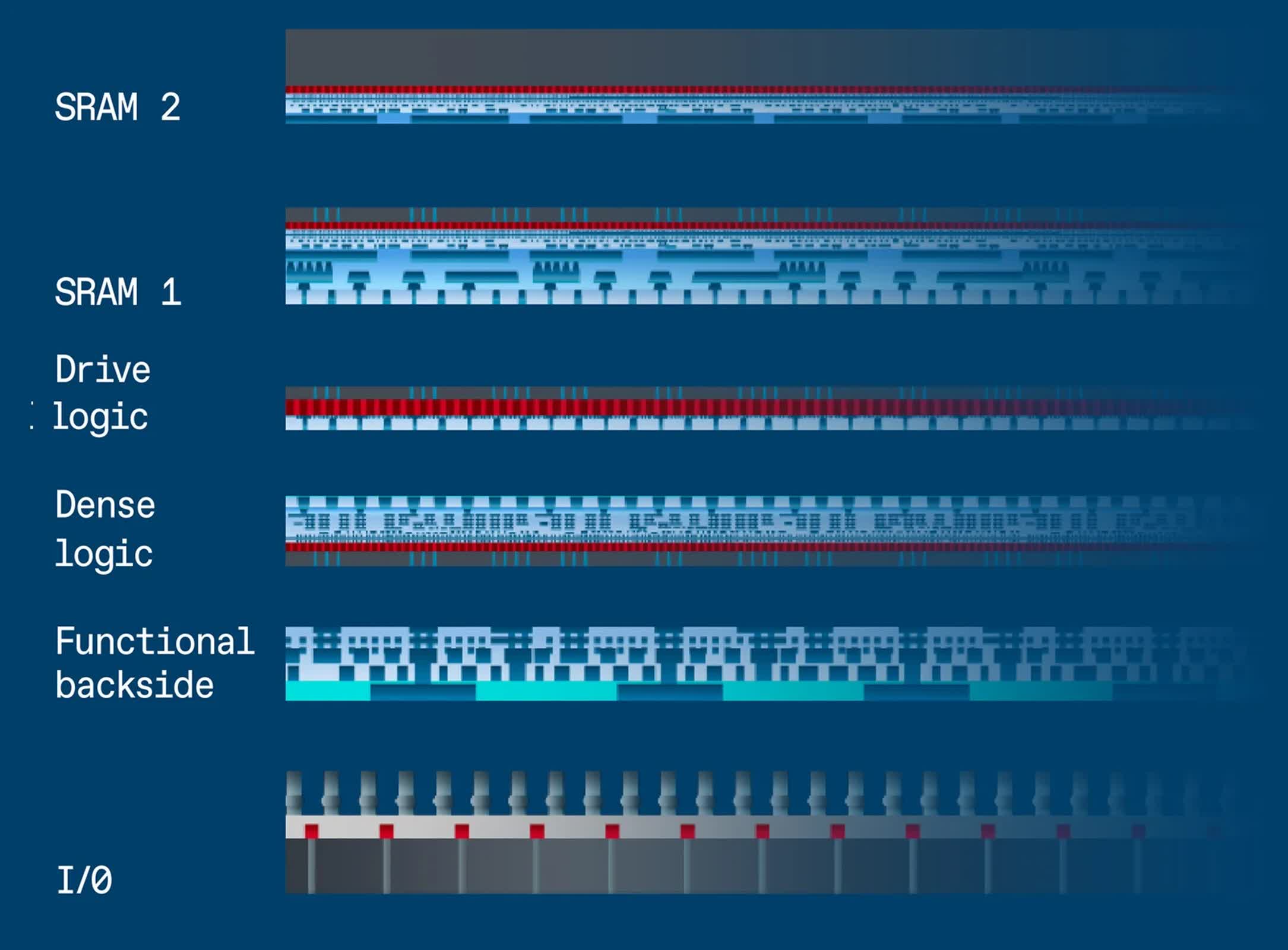
In the future, parts of chips will be made on their own silicon wafers using the appropriate process technology for each. They will then be 3D stacked to form SoCs that function better than those built using only one process technology. But engineers will have to carefully consider how heat flows through these new 3D structures.
These innovations are not without trade-offs. Thinning the silicon substrate to enable backside technologies can reduce its ability to dissipate heat, potentially creating new thermal hot spots. Simulations suggest that BSPDNs could increase local temperatures by as much as 14 degrees Celsius, highlighting the need for additional mitigation strategies.
These developments fall under what Imec refers to as the "CMOS 2.0" era, which is defined by advanced transistor architectures and specialized logic layers. By optimizing how signals are driven across the chip, these technologies aim to deliver improved performance and energy efficiency alongside potential gains in thermal management.
Still, the full thermal implications remain uncertain and demand thorough investigation as these technologies continue to evolve.
Myers warns that software-based approaches to thermal control, while useful, are inherently imprecise. They often throttle larger areas of a chip than necessary, which can unnecessarily reduce performance. Instead, he advocates for a holistic strategy known as system technology co-optimization, which integrates system design, physical layout, and process technology into a unified development process.
Myers concludes that by fostering collaboration across disciplines and leveraging advanced simulation tools, the industry can better anticipate and address the mounting thermal challenges facing future chips.


 English (US) ·