Serving tech enthusiasts for over 25 years.
TechSpot means tech analysis and advice you can trust.
Something to look forward to: In a modest laboratory tucked beneath the offices of Y Combinator in San Francisco, a young startup is working to upend one of the most entrenched technologies in chip manufacturing. Inversion Semiconductor, founded in 2024 by Rohan Karthik and Daniel Vega, is betting that shrinking particle accelerators down to tabletop size could unlock a new era of faster, more powerful semiconductor production.
Today, the world's most advanced chips are made with extreme ultraviolet (EUV) light, a technology dominated by Dutch giant ASML. Their machines use 13.5-nanometer light to etch impossibly fine patterns onto silicon wafers, but the process is slow, costly, and limited by the power of the light sources available. Inversion's founders believe they can leapfrog these constraints by harnessing a radically different approach: laser wakefield acceleration (LWFA).
LWFA is a technique that uses ultra-short, high-powered laser pulses to generate plasma waves. These waves can accelerate electrons to enormous energies over just a few centimeters, rather than the kilometers required by traditional particle accelerators like those at CERN.
The result is a compact device – 1,000 times smaller than conventional accelerators – that can, in theory, deliver up to 10 kilowatts of output power. That's not only far beyond what ASML's current systems can achieve, but also enough to potentially run multiple lithography machines at once or dramatically speed up the chipmaking process.
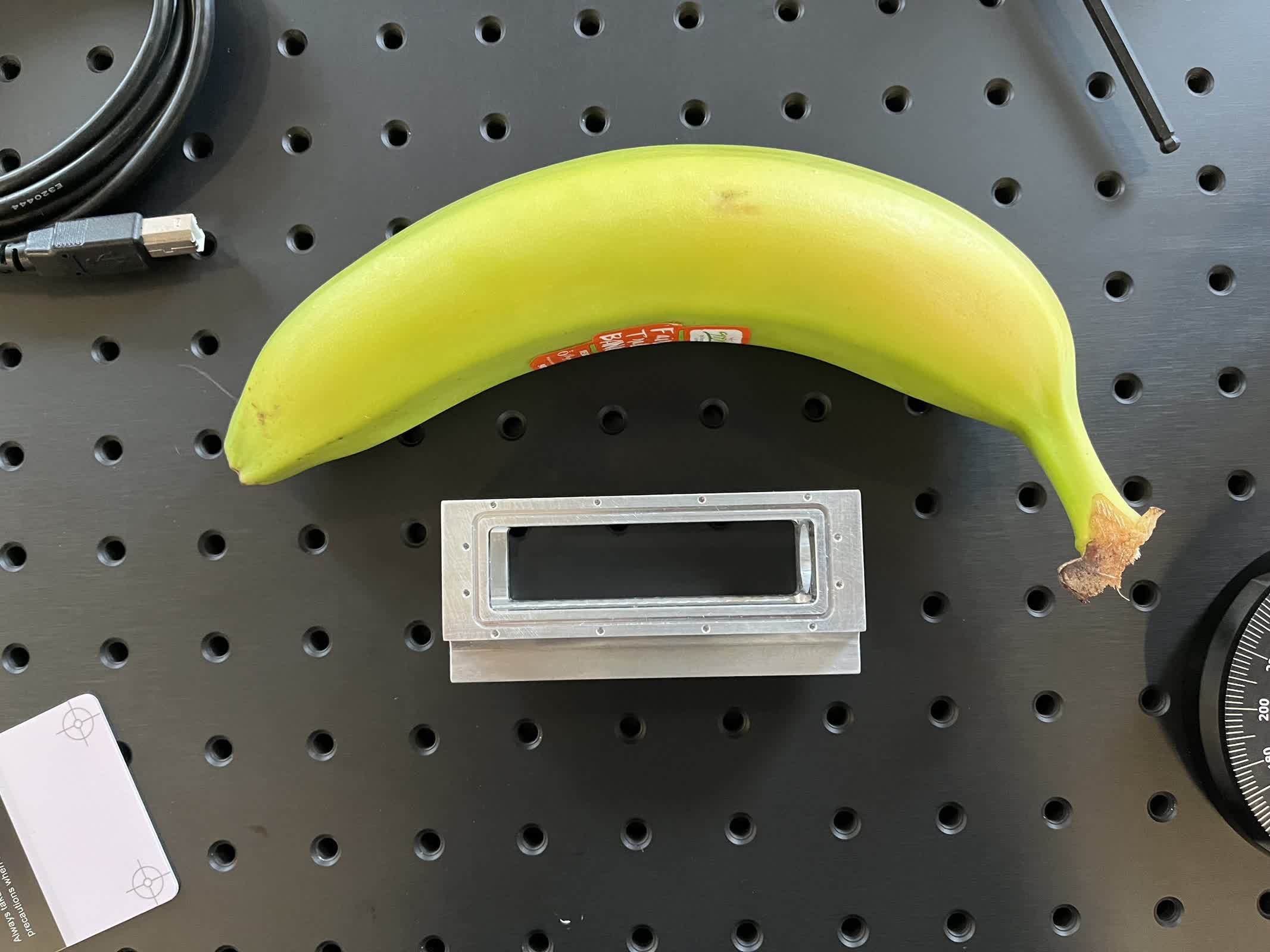
The company's immediate goal is to develop a tunable light source, dubbed Starlight, capable of producing 1 kilowatt of soft X-ray light in the 6 to 20 nanometer range. This output could serve applications ranging from industrial X-ray imaging to semiconductor mask inspection, and early interest has been expressed by major players such as Tesla and Applied Materials.
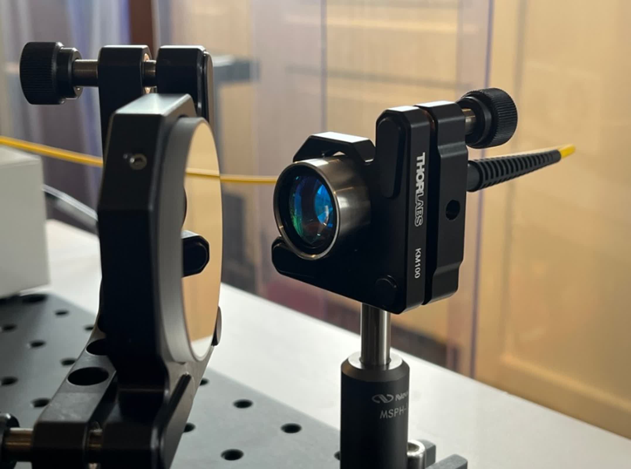
Inversion has also secured a partnership with the Lawrence Berkeley National Laboratory and the BELLA Center, collaborating on the BELLA-LUX project to refine laser stability and optimize light generation for semiconductor use.
But the path forward is fraught with technical and practical hurdles. The petawatt-class lasers needed for LWFA are themselves large, expensive, and notoriously difficult to keep running reliably for the 24/7 demands of modern chip fabs.
Maintaining stable, high-quality beams is essential for precise patterning, and even leading researchers acknowledge that LWFA-generated electron beams tend to have wide energy spreads and divergence, complicating their use for lithography.
There's also the challenge of integrating this new light source with existing lithography equipment. While using current EUV optics might be feasible at first, moving to even shorter wavelengths would require entirely new mirrors and supporting technologies, potentially forcing Inversion to build a whole new ecosystem from scratch.
Inversion's ambitions extend beyond just the light source. The company ultimately hopes to build complete lithography systems, directly challenging ASML's dominance. However, with no prior experience producing the highly reliable, mass-manufactured tools required by chipmakers, the startup faces significant skepticism about its ability to deliver on its promises.
Despite these obstacles, Inversion's founders remain undeterred. They see their technology as a way to break through the physical limits of current chipmaking and keep Moore's Law alive. If their compact accelerator can be made practical and affordable, it could transform not only semiconductor manufacturing but also a host of industries that rely on advanced light sources. For now, the company is focused on demonstrating its prototype system, LITH-0, powered by Starlight. The timeline for a fully functional, production-ready tool remains uncertain, but the race to shrink the particle accelerator – and with it, the future of chipmaking – is well underway


 English (US) ·