 8 months ago
19
8 months ago
19
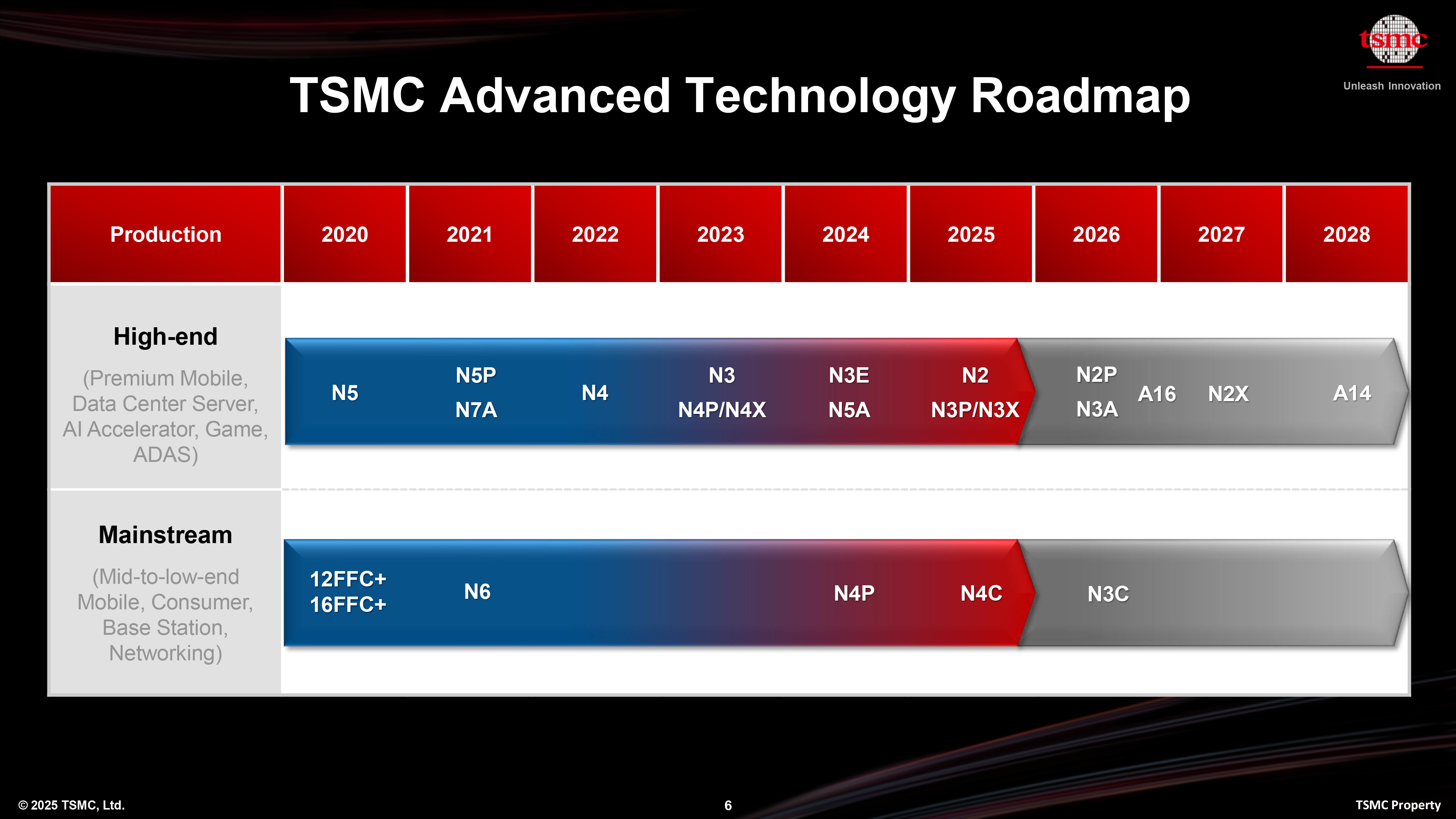
TSMC has revealed its A14 (1.4nm-class) manufacturing technology, which it promises will offer significant performance, power, and transistor density benefits over its N2 (2nm) process. At its North American Technology Symposium 2025 on Wednesday, the company disclosed that the new node will rely on its 2nd Generation gate-all-around (GAA) nanosheet transistors and will offer further flexibility with NanoFlex Pro technology. TSMC expects A14 to enter mass production in 2028 — but without backside power delivery. A version of A14 with backside power delivery is planned for 2029.
"A14 is our full-node next generation advanced silicon technology," said Kevin Zhang, senior vice president of business development and global sales and deputy COO at TSMC. "If you look at speed, enhancement [compared to N2] is up to 15%, power reduction is at 30%, logic density is 1.23x the overall chip density, or at least 1.2x [for mixed designs]. So, this is a very, very substantial technology."
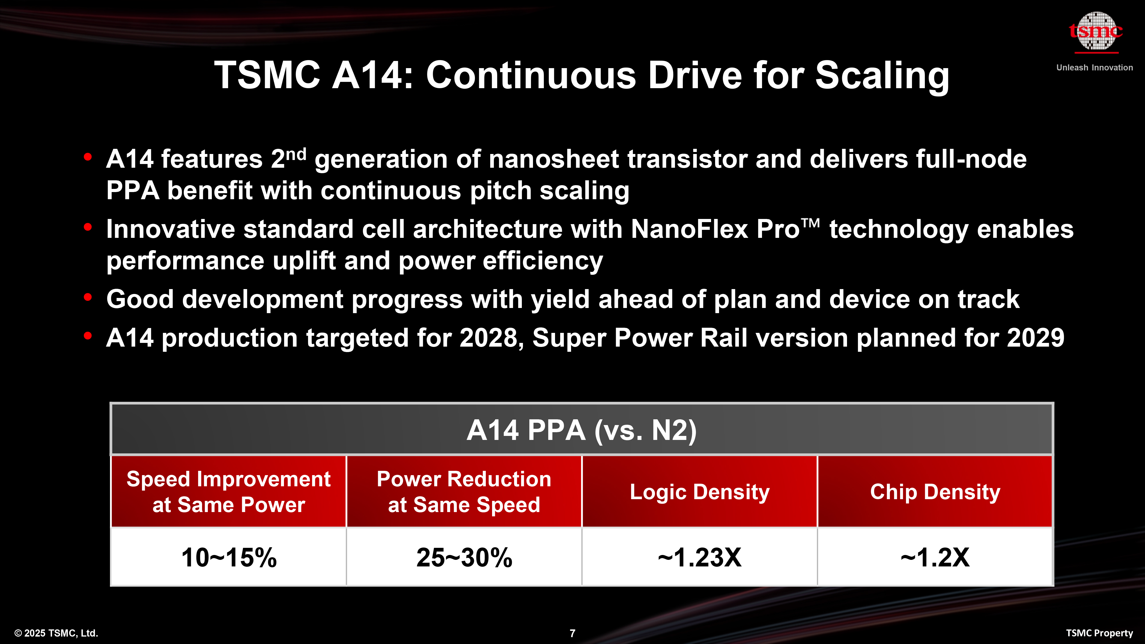
TSMC's A14 is brand-new process technology that is based on the company's 2nd Generation GAAFET nanosheet transistors and new standard cell architecture to enable performance, power, and scaling advantages. TSMC expects its A14 to deliver a 10% to 15% performance improvement at the same power and complexity, a 25% to 30% lower power consumption at the same frequency as well as transistor count, and 20% - 23% higher transistor density (for mixed chip design and logic, respectively), compared to N2. Since A14 is an all-new node, it will require new IPs, optimizations, and EDA software than N2P (which leverages N2 IP) as well as A16, which is N2P with backside power delivery.
Advertised PPA Improvements of TSMC's New Process Technologies
Swipe to scroll horizontally
| Row 0 - Cell 0 | A16 vs N2P | N2X vs N2P | A14 vs N2 | A14 SPR vs N2 |
Power | -15% ~ -20% | lower | -25% ~ -30% | lower |
Performance | 8% - 10% | 10% | 10% - 15% | higher |
Density* | 1.07x - 1.10x | ? | 1.2x | denser |
Transistor | GAA | GAA | 2nd Gen GAA | 2nd Gen GAA |
Power Delivery | SPR | Front-side w/ SHPMIM (?) | Front-side w/ SHPMIM (?) | SPR |
HVM | H2 2026 | 2027 | 2028 | 2029 |
*Chip density published by TSMC reflects 'mixed' chip density consisting of 50% logic, 30% SRAM, and 20% analog.
**At the same area.
***At the same speed.
Unlike A16 (and just like N2 and N2P), A14 lacks Super Power Rail (SPR) backside power delivery network (BSPDN), which enables the technology to target applications that do not get tangible benefits from BSPDN — which comes at additional cost. There are plenty of client, edge, and specialty applications that can take advantage of the extra performance, lower power consumption, and transistor density enabled by TSMC's 2nd Generation GAA nanosheet transistors, but that do not need dense power wiring and are fine with a traditional front side power delivery network.
"The technology also features our […] NanoFlex Pro technology, [which is really] design technology co-optimization (DTCO) allowing designer to design their product at a very flexible fashion, allow them to achieve optimum power performance benefit," Zhang said. "This technology is going into production by 2028. The first version of this technology does not have the backside power rail."
Of course, TSMC understands the needs of its customers that develop high-performance client and data center applications, so it plans to offer A14 with SPR backside power delivery in 2029. For now, the company did not disclose the exact name of the process technology, though it is reasonable to expect it will be called A14P, following TSMC's traditional nomenclature. Going forward, expect A14 to get its max performance (A14X) and cost-optimized (A14C) versions sometimes after 2029.
One of the key advantages of TSMC's A14-series process technologies will be the company's NanoFlex Pro architecture, which will enable chip designers to fine-tune transistor configurations to achieve optimal power, performance, and area (PPA) for specific applications or workloads. With non-Pro FinFlex, developers can mix and match cells from different libraries (high performance, low power, area efficient) within one block to optimize performance, power, and area. TSMC has not disclosed explicit technical details differentiating NanoFlex from NanoFlex Pro, so we can only wonder whether the new version allows for more granular controls over cells — or even transistors — or whether it will offer better algorithms and software enhancements to enable faster exploration and optimization of transistor-level trade-offs.
TSMC's target for production of chips on its A14 process technology is 2028, though it refrained from mentioning if it would commence high volume manufacturing on A14 in the first or second half of the year. Considering the fact that A16 and N2P will kick off HVM in the second half of 2026 (i.e., late 2026), with chips on the market in 2026, we have a feeling that A14 is targeted for the first half of 2028 — on track to serve client applications due in the second half of the year.


 English (US) ·