 6 months ago
37
6 months ago
37
As TSMC is gearing up to start making chips on its N2 (2nm-class) process technology later this year, rumors have emerged regarding the pricing of N2 wafers, as well as the pricing of subsequent nodes. We already knew that TSMC reportedly plans to charge up to $30,000 per wafer processed using its N2 technology, but now Taiwan-based China Times reports that the company will charge up to $45,000 per wafer for 'more advanced nodes,' which allegedly points to the company's A16 (1.6nm-class) node.
2nm production is expensive
"TSMC's wafer foundry price for 2nm chips has soared to $30,000 per wafer, with [more] advanced nodes rumored to reach up to $45,000," the report by China Times reads. This claimed price is 45% higher than the rumored cost of TSMC's N2 node, which is also rumored to have risen up to $30,000.
There are a few things you need to know about pricing at TSMC and other contract chipmakers. First up, pricing at foundries is heavily dependent on production volumes and the client.
Apple, being the largest customer of TSMC's most advanced process technologies, is believed to pay less than its industry peers for wafers. When it comes to other clients like AMD, Intel, Nvidia, and Qualcomm, their pricing depends on overall volumes, in addition to the proportion of that volume being based on a client's uptake of leading-edge nodes.
So, bear in mind that all reported quotes on TSMC's (or any foundry's) wafers are approximate at best. It certainly goes without saying that TSMC does not comment on pricing and volumes. So, the only points of comparison are other unofficial prices.
Swipe to scroll horizontally
A16 | $45,000 | 2026 H2 |
N2 | $30,000 | 2025 H2 |
N3 | $18,000 - $20,000 | 2022 H2 |
N5 | $16,000 | 2020 |
N7 | $10,000 | 2018 |
N10 | $6,000 | 2016 |
N28 | $3,000 | 2014 |
40nm | $2,600 | 2008 |
90nm | $2,000 | 2004 |
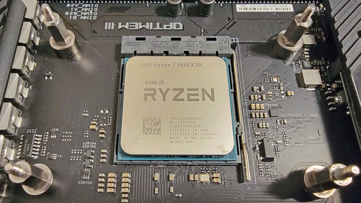
Several major chip developers are transitioning to 2nm technology. AMD recently confirmed that it had produced the first silicon for its next generation of EPYC server processors codenamed Venice, so did Fujitsu. The report says that MediaTek is scheduled to finalize its design work for its next-generation mobile system-on-chip (SoC) on TSMC's N2 node shortly. Qualcomm is also reportedly developing the third generation of its Snapdragon 8 Elite mobile platform on the same node.
Apple is expected to be among the first to adopt N2, though the company has not formally confirmed this. If this is the case, expect next-generation A20-series and M6-series processors to rely on the N2 node, though that's an educated guess on our part.
TSMC will ramp up production of N2-based chips later this year at two fabs more or less simultaneously, which is a rather unprecedented event (more on this later). The report claims that TSMC’s internal targets for 2nm indicate a monthly production capacity of around 30,000 wafers by the end of this year.
Flip a wafer, bump the price?
While the alleged pricing of $30,000 per N2 wafer seems like a lot, the $45,000 for a 'more advanced' node seems a bit overwhelming. The report does not specifically mention A16 process technology, but since it is too early to discuss pricing of A14 and more advanced manufacturing nodes, it's very likely that the report points to the pricing of wafers processed using TSMC's 1.6nm-class technology.
You should take the $45,000 quote with a grain of salt. As we mentioned earlier, different customers pay different prices. But we can still speculate about why A16 wafers are rumored to be much more expensive than their N2 counterparts.
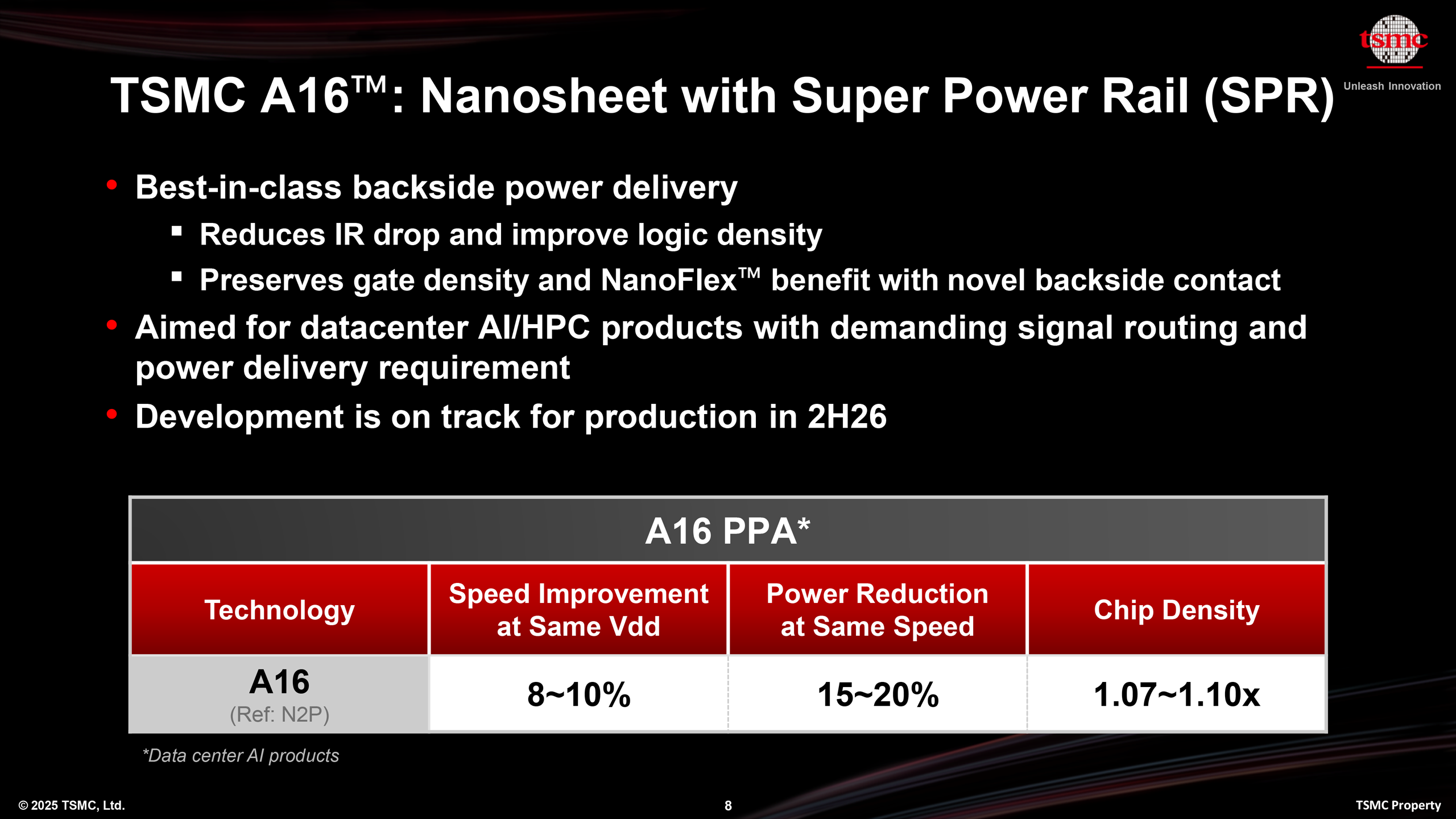
The reason might be simple: unlike N2 and N2P, A16 supports backside power delivery network (BSPDN) that is particularly useful for big near-reticle-sized processors aimed at AI and HPC applications, but is fairly expensive to produce.
The production of a BSPDN requires several additional steps in the manufacturing process, which significantly affect pricing.
First, chip fabrication proceeds as usual: transistors are built on the front side of a silicon wafer using traditional steps like deposition, lithography, etching, and doping to form the active devices. Once the transistors are built, the wafer is bonded face-down onto a blank carrier wafer using hybrid bonding techniques.
Then, the original wafer is carefully thinned out from the back side through grinding and chemical-mechanical polishing, reducing the silicon thickness to just a few micrometers, exposing the bottom of the active transistor layer.
Now that the backside is exposed, new metal interconnects dedicated solely to power delivery are deposited. TSMC uses the most efficient implementation of a BSPDN, but it's also the most difficult to produce.
The BSPDN connects thick copper lines to reduce resistance directly to transistors. After backside processing, the wafer proceeds through standard packaging steps.
The separation of power and signal wiring improves overall chip performance due to better power delivery, reducing voltage drops and freeing up space on the front side for faster signal routing.
However, the cost of backside power delivery will limit its usage to companies developing large and expensive processors, such as next-generation AI and HPC GPUs, which are expected to consume kilowatts of power and which greatly benefit from BSPDN.
Extreme development costs
The report claims that the development of a single 2nm chip is projected to cost approximately $725 million, which is a lot, and limits the usage of the technology to a handful of companies. However, there is a catch.
The eye-watering $725 million figure likely involves the development of a whole platform that relies on that particular technology and includes multiple chips.
For example, the list of Apple's products relying on TSMC's N3 process technologies includes nine products for now, including A17 Pro, A18, A18 Pro, M3, M3 Pro, M3 Max, M4, M4 Pro, and M4 Max. Eventually, that list will likely expand with N3P-based A19, A19 Pro, M5, M5 Pro, and M5 Max.
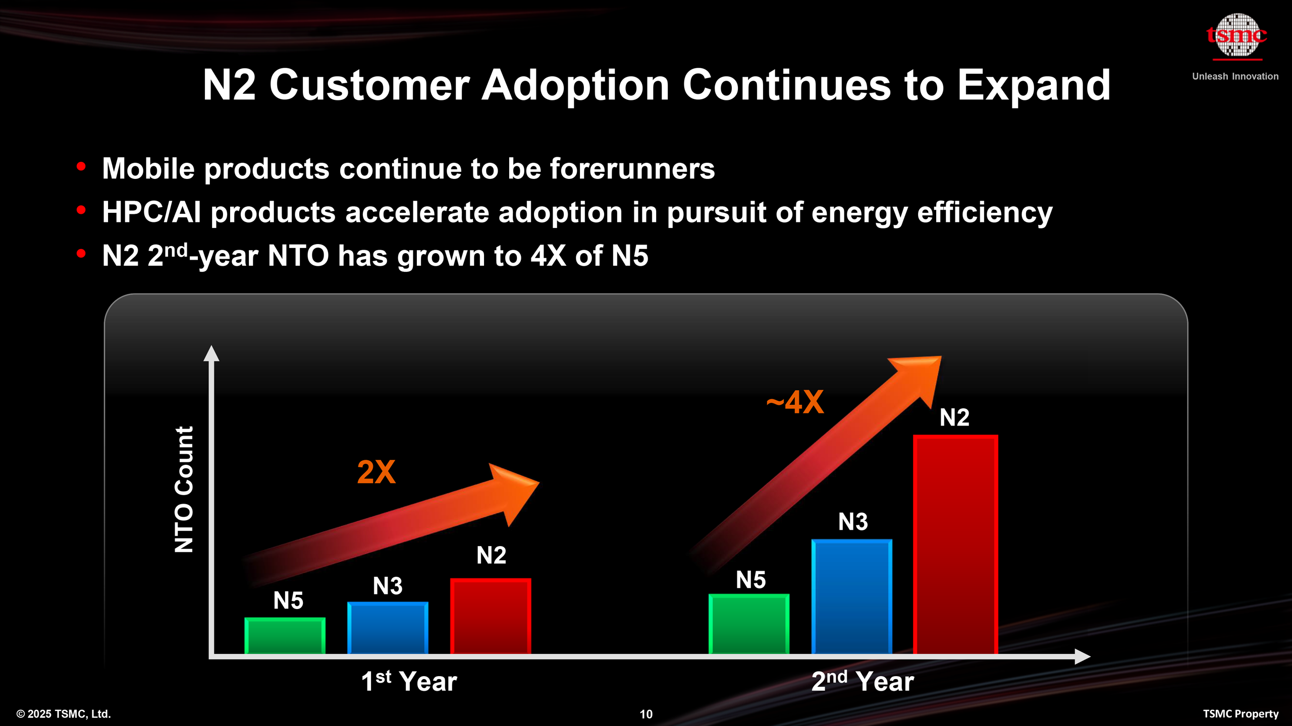
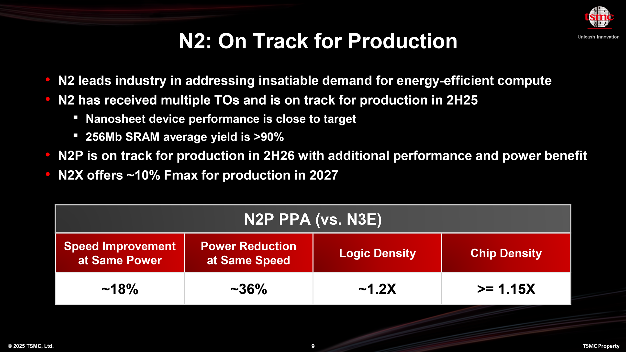
Despite the rather extreme upfront cost, the number of new tape-outs in the second year of production is expected to be four times greater compared to what was achieved during a similar stage with N5. This factor highlights the importance of leading-edge nodes to multiple companies developing chips for AI, HPC, client computers, and smartphones.
To meet soaring demand for its N2 process technology and other nodes in the same process design kit (N2P, A16, N2X, etc.), TSMC is prepping its two N2-capable production facilities in Hsinchu and Kaohsiung. Eventually, the company will build additional N2-capable fabs in Taiwan and the USA.
Industry observers expect that this node could achieve record-setting capacity ramp-up speeds due to intense customer interest. TSMC itself is optimistic about AI accelerators driving future revenue, forecasting a five-year compound growth rate approaching the mid-40% range starting in 2024.
Follow Tom's Hardware on Google News to get our up-to-date news, analysis, and reviews in your feeds. Make sure to click the Follow button.


 English (US) ·