 7 months ago
75
7 months ago
75
Intel explained the rationale behind its High-NA EUV strategy at its Intel Foundry Direct 2025 conference this week. Despite persistent questions around cost-effectiveness, Intel has championed its use of the new High-NA EUV chipmaking tool with its forthcoming 14A process. However, Intel has not yet fully committed to using the new tool in production, but it has an alternative production flow of its 14A node that uses standard Low-NA EUV as a backup plan.
Intel has already received a second high-NA EUV tool, installed in its Oregon fab, and the company says the technology is progressing well. However, due to continuing development, the ~$400 million ASML Twinscan NXE:5000 High-NA EUV machines haven’t been used in a production environment yet, so Intel isn’t taking any risks.
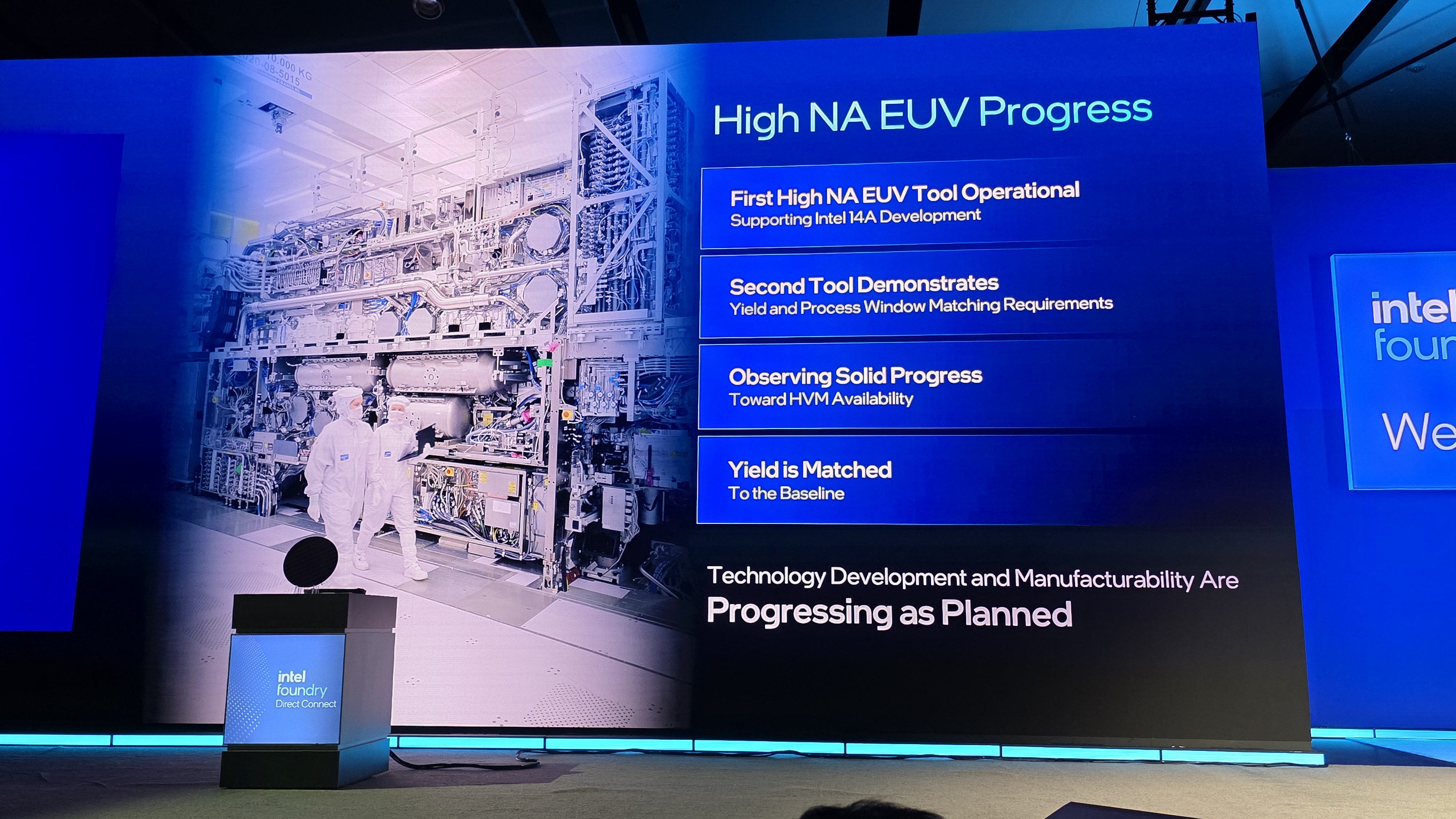
“[..]The first one is, Intel still has the option to have either a Low-NA or a High-NA solution on our 14A technology, and its design-rule compatible, there will be no impact to the customers, depending on the path that we choose. Second, High-NA EUV is performing to the expectations, and we will introduce it at the right time," said Dr. Naga Chandrasekaran, EVP, CTOO & GM of Intel Foundry Technology and Manufacturing.
"We already have data on 18A as well as 14A that shows yield parity between our Low-NA-based solution and a High-NA-based solution. So, we are continuing to make progress on the technology front and ensuring that we have the right options available for us to make sure the solution we deliver to our customers has the lowest risk and the best reward in terms of the decisions we make,” Naga explained.
Intel will only use High-NA EUV on a small number of layers of the 14A node (the exact number isn’t known), while other machines of varying resolutions will be used for the other layers. That means the decision between the two machines will only impact a select portion of the manufacturing process, but Intel says using triple-patterning with a Low-NA EUV (more below) machine instead of High-NA produces the same results.
Because both techniques are design-rule compatible, Intel’s customers won’t have to change their designs regardless of the company’s decision on the final manufacturing flow, either with or without High-NA EUV, which helps defray concerns that customers might have with Intel embracing an as-yet unproven production technology.
Additionally, Intel’s claim that both production flows offer the same yields signals that there won’t be severe time-to-market repercussions if High-NA EUV development hits a snag, or if Intel chooses not to deploy it due to economics. Employing multipatterning often reduces yields, but Intel's claim of yield parity speaks to the advances of modern multipatterning, particularly in the field of overlay technology.
Most of the public-facing conversations about High-NA EUV have centered around cost, there's plenty of industry speculation that High-NA isn't as cost-effective as multi-patterning with Low-NA EUV, but there are still numerous technological hurdles to bringing the machines into production. Most of the challenges center around the universe of complementary technologies required to make High-NA viable, like resists, photomasks, and computational lithography, among others, which have to be optimized for the new machines.
However, Intel adopted ASML's machine first to get a leg up on the competition, and it has already produced 30,000 wafers using High-NA lithography during the development phase. As a representative explained later in the event, Intel still sees significant cost savings due to eliminating around 40 process steps.
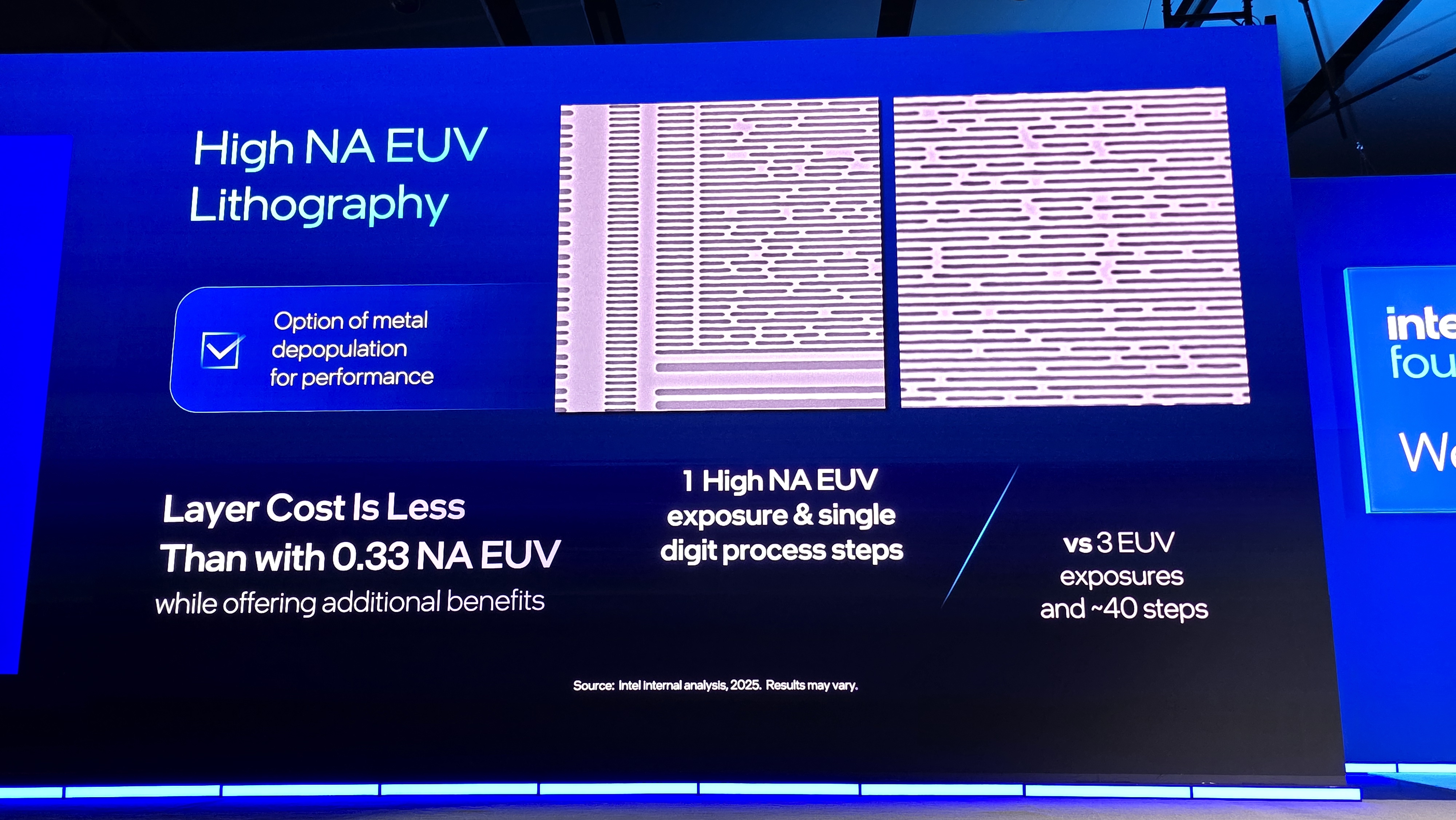
“Finally, I want to talk about High-NA EUV. Why do we do this? It's very simple; It's lower cost. In the middle picture, you see a pattern that has been generated by a single pass High-NA EUV and a pitch that is comparable to the pitch that we need for 14A. The right-hand side shows a very similar pattern generated with a traditional approach, where we use three EUV exposures [triple patterning], and overall about 40 process steps to generate this pattern."
"So, overall, we see much shorter, simpler flow, and this is the type of application where we use High-NA in 14A, which reduces the cost compared to the multi-pass 0.33 NA EUV [Low-NA]. Additionally, this provides the option to de-populate the metal layers and get additional performance enhancement.”
Intel didn't specify whether or not its comparisons are based on a full-reticle-sized print. High-NA can only print half of a reticle at a time, requiring two prints to create one reticle-sized processor and relying upon stitching to bring the two prints together into a single cohesive unit. In contrast, die that are equal to or smaller than a half-reticle size will only require one print with High-NA EUV. In contrast, Low-NA EUV machines can process a full reticle-sized die in a single pass.
Thoughts
Intel has plenty of scar tissue from its 10nm node failures that ultimately ended in the company losing its chipmaking lead over TSMC, and it chalks the 10nm issues up to making too many big bets on new manufacturing techniques and technologies at once.
The decision to develop an alternative Low-NA production flow is designed to prevent repeating those past mistakes, and Intel has also de-risked other types of advances by developing alternative solutions in the past.
For instance, the company developed its new backside power delivery system with the 18A node, an industry first, while simultaneously developing gate-all-around (GAA) transistors, a first for Intel. To ensure a backup plan, the company employed a more robust de-risking strategy with its 18A process that included developing an internal-only trial process node without backside power. However, development went well with both GAA and backside power delivery, so Intel pushed forward with the full version of the 18A node.
Intel rival TSMC has confirmed it will not use High-NA with its competing A14 node, and it hasn't indicated when it will employ the new High-NA EUV tool in volume production. Intel had originally planned to use High-NA with its 18A process, which arrives before the 14A node. Intel later changed those plans, saying that the process node's unexpectedly fast development meant the machines wouldn't be ready in time.


 English (US) ·